Universal array type probe card design for semiconductor device testing

a technology of semiconductor devices and probe cards, applied in the field of test probe systems, can solve the problems of expensive items that must be purchased anew, labor-intensive and time-consuming process, and the hardware change and verification process is labor-intensive and time-consuming

Active Publication Date: 2012-08-21
TAIWAN SEMICON MFG CO LTD
View PDF10 Cites 18 Cited by
  • Summary
  • Abstract
  • Description
  • Claims
  • Application Information

AI Technical Summary

Problems solved by technology

The new test configuration must be verified before the new semiconductor device can be tested and the hardware change and verification process is a labor intensive and time consuming process.
Moreover, since...

Method used


Image

  • Universal array type probe card design for semiconductor device testing
  • Universal array type probe card design for semiconductor device testing
  • Universal array type probe card design for semiconductor device testing

Examples


Embodiment Construction

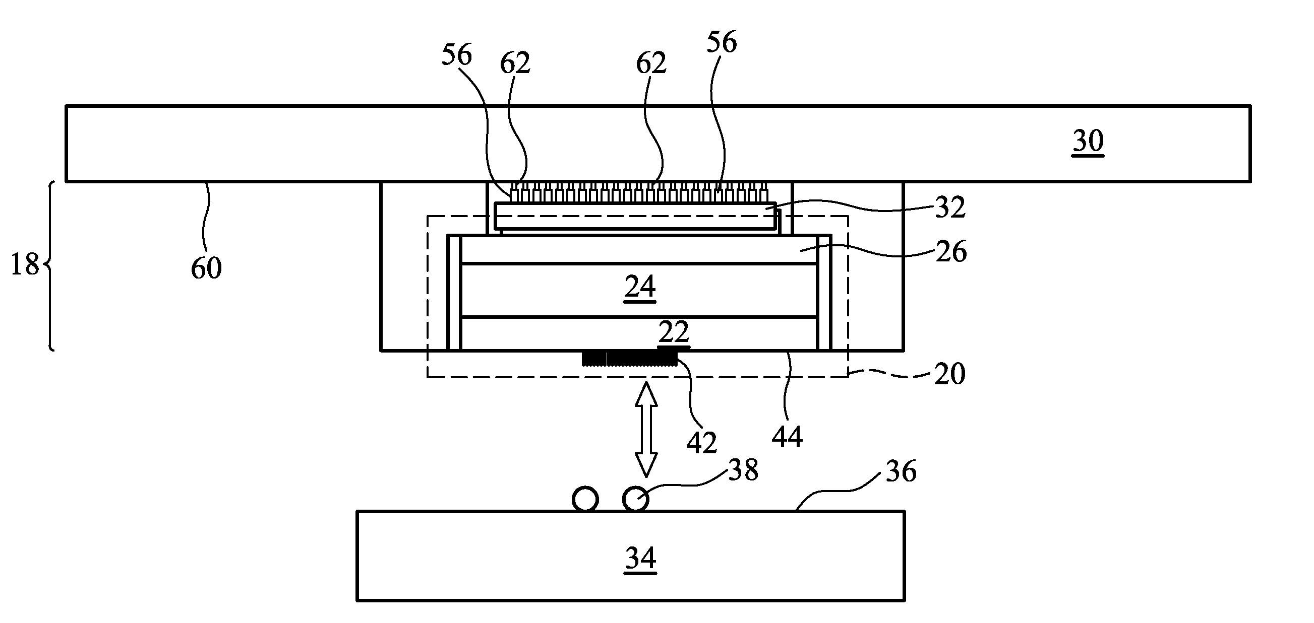
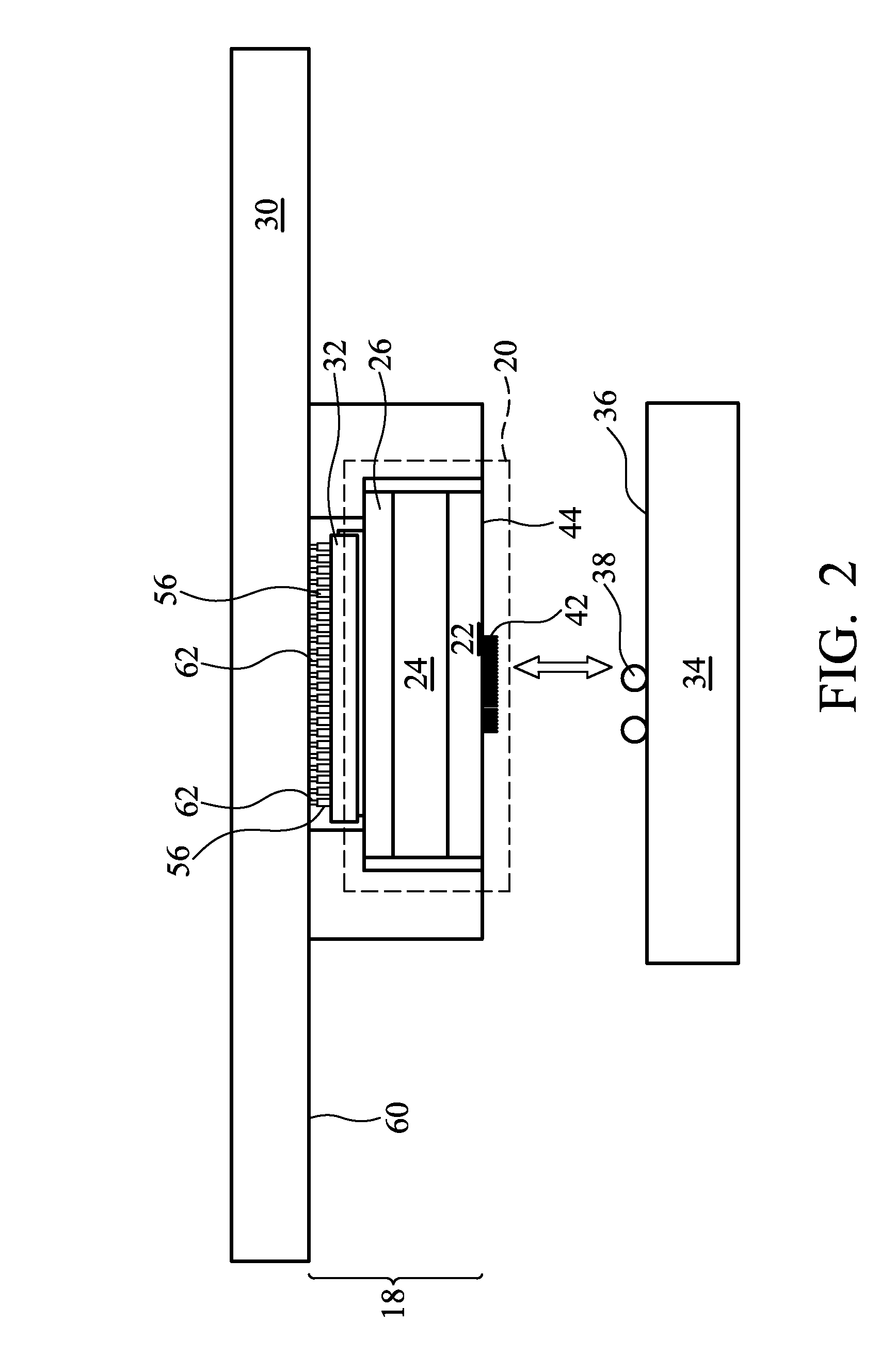
[0017]Provided is a universal probe assembly. The probe head assembly may be usable in various electrical test assemblies, i.e., test equipment used for conducting functional, electrical and / or parametric testing of finished semiconductor devices. Test equipment with various test assemblies are available from multiple manufacturers and are commercially available. Provided is a test assembly that includes a printed circuit board, PCB, used for testing an associated semiconductor device and a probe head from which a plurality of probes extend, the probes forming a probe pattern. The probes contact a test pattern formed on a semiconductor device formed on a semiconductor wafer, to test the semiconductor wafer. The contacts of the test pattern may be bumps, pads or other suitable conductive contacts. The probe head is also coupled to the PCB via a plurality of contacts arranged in a contact pattern. According to one aspect, a universal probe pattern is provided. The universal probe patt...


PUM


Abstract

A universal system for testing different semiconductor devices provides a probe head with a probe pattern that may be used to test different test patterns formed on different semiconductor devices. Each of a plurality of bumps or pads of the test pattern contacts a corresponding probe of the probe head to enable the semiconductor device to be tested. The universal probe head may additionally or alternatively include a substrate design on the probe head that provides a pattern on the substrate of the probe head that may be used in conjunction with different patterns formed on a plurality of different printed circuit boards for testing different semiconductor devices.

Description

FIELD OF THE INVENTION[0001]The present invention relates to test probe systems for electrically testing semiconductor devices.BACKGROUND OF THE INVENTION[0002]Semiconductor devices are used in countless applications throughout the world and millions upon millions of individual semiconductor devices are produced annually. Each semiconductor device must be individually and completely electrically tested before it is installed within an electronic or other device. Different semiconductor devices perform different functions and therefore undergo different functional, parametric and electrical tests. In any semiconductor device fabrication or testing facility, the number of different semiconductor devices to be tested far exceeds the number of test equipment available to test the devices. As such, different semiconductor devices are tested on the same test assembly. The test assembly typically includes a probe head with probes or pins that contact the pattern formed on the semiconductor...

Claims


Application Information

Patent Timeline
IPC IPC(8): G01R31/20G01R31/02
CPCG01R1/07371
Inventor CHENG, HSU MINGKUO, YUNG-LIANGLEE, PI-HUANGLUH, ANNHWANG, FRANKWU, WEN-HUNG
Owner TAIWAN SEMICON MFG CO LTD
Why Eureka
Try Eureka