Method and structure for manufacture of light emitting diode devices using bulk GaN

a light-emitting diode and bulk gan technology, applied in the direction of semiconductor devices, basic electric elements, electrical apparatus, etc., can solve the problems of inapplicability, inability to achieve separation based on conventional methodologies previously described, and inability to enable a short optical cavity length, etc., to achieve cost saving, increase the effect of radiative recombination efficiency and higher iqe of devices

Active Publication Date: 2012-08-28
SLT TECH
View PDF58 Cites 198 Cited by
  • Summary
  • Abstract
  • Description
  • Claims
  • Application Information

AI Technical Summary

Benefits of technology

[0014]One or more benefits may be achieved in the specific embodiments. In particular, the use of a short optical cavity length will minimize re-absorption of emitted light in LEDs. This is important for devices on state-of-the-art crystalline substrate materials containing at least one of GaN, AlN or InN, as depending on the growth method utilized to fabricate the crystalline substrate material (for example hydride vapor phase epitaxy or ammonothermal growth, among others), impurity levels can remain substantially high. This leads to crystalline materials which are not perfectly optically transparent, thus minimizing the thickness of this material through which light is emitted is advantageous. As shown in FIG. 2, enhanced performance has been demonstrated for conventional heteroepitaxial devices employing a short optical cavity length as compared to devices emitting through a sapphire substrate. In the case of an LED device fabricated on bulk crystalline substrate material containing at least one of GaN, AlN, or InN, this effect could be even more significant due to higher absorption properties in the bulk crystalline material as opposed to low-impurity substrates such as sapphire.
[0017]One or more benefits can be achieved by utilizing this alternative method and structure, in particular the fact that this method is not destructive to the substrate. This is of importance given that the current cost of bulk crystalline substrate material containing at least one of GaN, AlN, or InN is significantly prohibitive to any near-term industry adoption of LED technology based on such bulk crystalline substrates. It is anticipated that cost savings would be realized if a method and process flow were developed which allowed the crystalline substrate material to remain intact. Conceivably re-use or multiple uses of the same crystalline substrate material would be possible after appropriate re-finishing in one or more embodiments.
[0018]In one or more preferred embodiments, the orientation of the crystalline substrate material containing at least one of GaN, AlN, or InN, is nonpolar or semipolar. There are one or more substantial benefits which can be realized using the novel orientations in these embodiments, in particular due to the reduction or absence of internal electric fields in the device. For example, this allows for increased radiative recombination efficiencies, and therefore higher IQE in devices in these orientations. Devices in these orientations also allow for use of thicker quantum wells in the active region without a performance trade-off due to internal fields. Additional benefits in these orientations include the potential for increased indium incorporation,xi and therefore the potential for light emission at longer wavelengths than conventional GaN-based devices, and potentially across the entire visible spectrum. Additionally, benefits include improved carrier distribution due to a predicted lower hole effective mass,xii,xiii the potential for higher hole concentrations in p-type material,xiv improved temperature stability, and potential for highly polarized light emission, among other benefits. Promising device demonstrations, in particular out of research groups at the University of California at Santa Barbara (i.e. References 1-8), have validated one or more of these potential benefits of devices on various nonpolar and semipolar orientations of GaN.

Problems solved by technology

Techniques and methods that are applied to commercial heteroepitaxial LEDs (grown on non-native substrate materials) to achieve high extraction efficiencies are either largely unavailable or inapplicable without considerable modification in the case of LEDs on bulk-GaN substrates, or substrates which substantially comprise at least one of GaN, AlN, or InN materials.
Thus, effecting a separation based on conventional methodologies previously described is not possible in order to enable a short optical cavity length.

Method used


Image

  • Method and structure for manufacture of light emitting diode devices using bulk GaN
  • Method and structure for manufacture of light emitting diode devices using bulk GaN
  • Method and structure for manufacture of light emitting diode devices using bulk GaN

Examples


Embodiment Construction

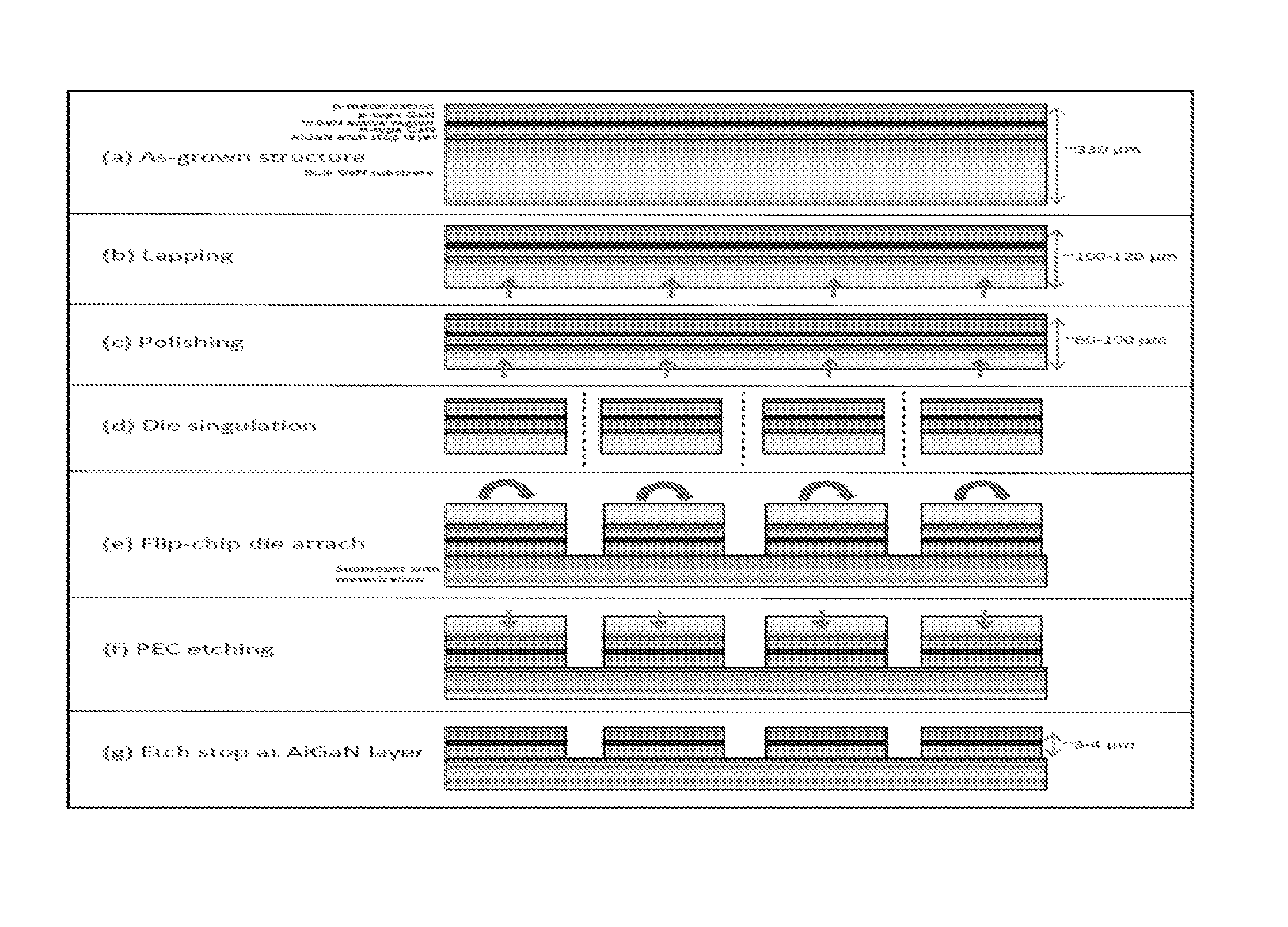
[0024]In one or more specific embodiments, the present invention provides a variety of different process configurations and structures, with a desire of developing a robust, high-extraction-efficiency LED platform designed specifically around high-internal quantum efficiency (IQE) LED devices on bulk-GaN substrates. As previously discussed, the primary technical challenge in implementing existing high-extraction device configurations using bulk-GaN substrates or related bulk nitride-containing substrates, is transitioning from the epilayer-plus-substrate thickness of crystalline material to a reduced thickness of crystalline material (just 3-4 um or 200 nm to 5 micrometers) according to a specific embodiment). In a specific embodiment, a surface texturing step can be added to the present method and structure to increase light extraction efficiency.

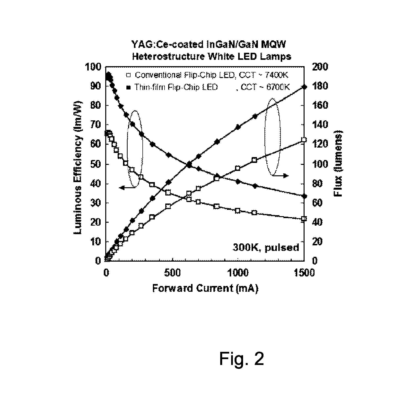
[0025]FIG. 2 is a simplified plot of light output and luminous efficiency vs. current comparisons between white LED lamps based on YAG:Ce...


PUM

PropertyMeasurementUnit
thicknessaaaaaaaaaa
thicknessaaaaaaaaaa
thicknessaaaaaaaaaa

Abstract

A method for manufacturing a plurality light emitting diodes includes providing a gallium nitride containing bulk crystalline substrate material configured in a non-polar or semi-polar crystallographic orientation, forming an etch stop layer, forming an n-type layer overlying the etch stop layer, forming an active region, a p-type layer, and forming a metallization. The method includes removing a thickness of material from the backside of the bulk gallium nitride containing substrate material. A plurality of individual LED devices are formed from at least a sandwich structure comprising portions of the metallization layer, the p-type layer, active layer, and the n-type layer. The LED devices are joined to a carrier structure. The method also includes subjecting the gallium nitride containing bulk crystalline substrate material to at least one etching process to selectively remove crystalline material underlying the etch stop layer, wherein the etch stop layer is exposed, and the etch stop layer remains substantially intact.

Description

CROSS-REFERENCES TO RELATED APPLICATIONS[0001]This application claims priority to U.S. Provisional Application No. 61 / 164,407 filed Mar. 28, 2009, commonly assigned, and incorporated by reference in its entirety for all purpose herein.BACKGROUND OF THE INVENTION[0002]Gallium nitride (GaN) based solid-state lighting technologies have made advances in the past three decades and promise to replace traditional fluorescent and incandescent bulbs for general illumination at tremendous energy and cost savings. GaN-based high-brightness light-emitting diodes (LEDs) have already penetrated various markets such as displays, traffic signals, cell phone backlights, and automotive lighting, and white LEDs have presence in various niche lighting markets. The efficiencies of such commercially available white LEDs have surpassed that of incandescent lighting and are now competitive with that of fluorescent lamps (˜70-100 lumens per Watt (lm / W)). However, the performance of individual LED components...

Claims


Application Information

Patent Timeline
Patent Type & Authority Patents(United States)
IPC IPC(8): H01L21/30
CPCH01L33/007H01L33/0095H01L33/0079H01L33/0093
Inventor POBLENZ, CHRISTIANESCHMIDT, MATHEW C.FEEZELL, DANIEL F.RARING, JAMES W.SHARMA, RAJAT
Owner SLT TECH
Why Eureka
Try Eureka