Semiconductor device, semiconductor package, interposer, semiconductor device manufacturing method and interposer manufacturing method
a semiconductor device and manufacturing method technology, applied in the manufacture of printed circuits, printed circuit aspects, basic electric elements, etc., can solve the problems of difficult to achieve the above two conventional techniques, difficult to disconnect wires, and often occur solder resist cracks, so as to reduce the possibility of disconnection of interconnect wires passing between external coupling terminals in the interposer
- Summary
- Abstract
- Description
- Claims
- Application Information
AI Technical Summary
Benefits of technology
Problems solved by technology
Method used
Image
Examples
first embodiment
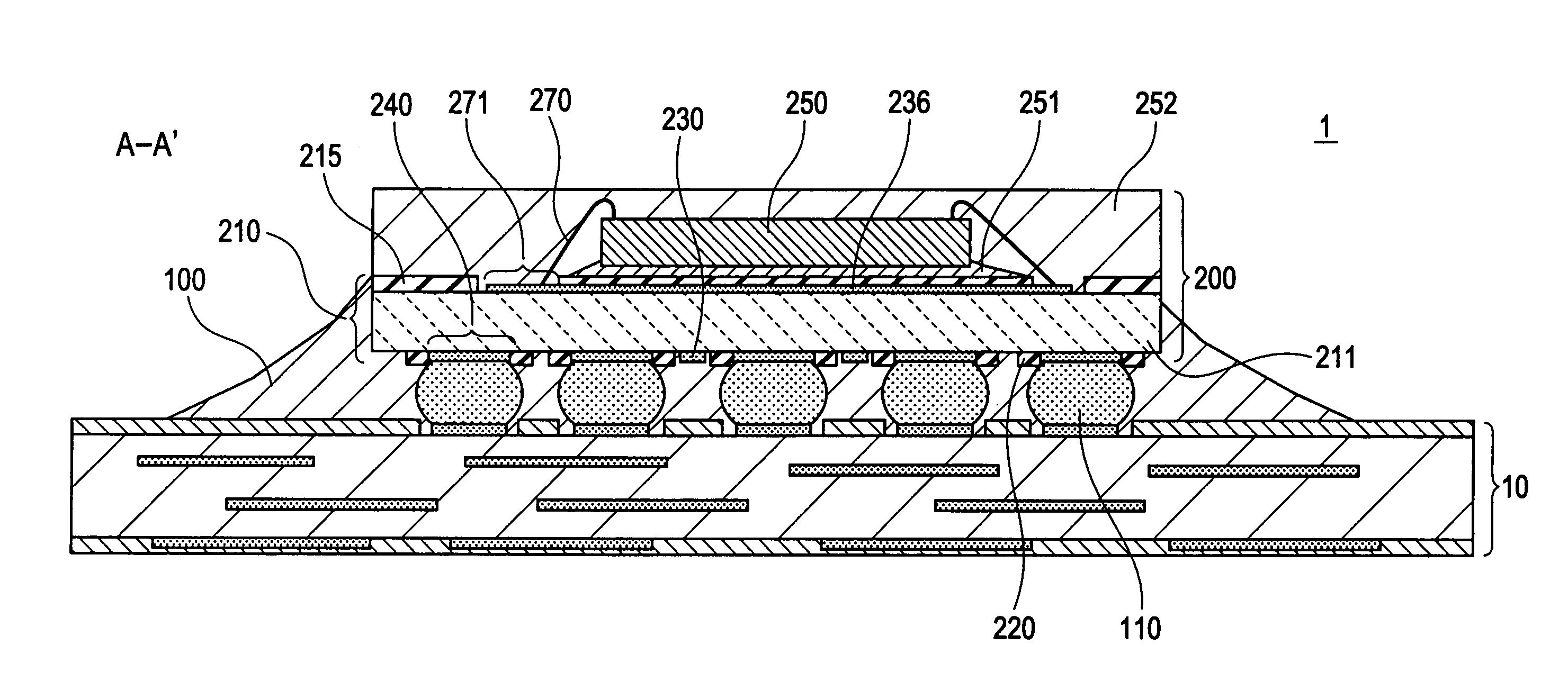
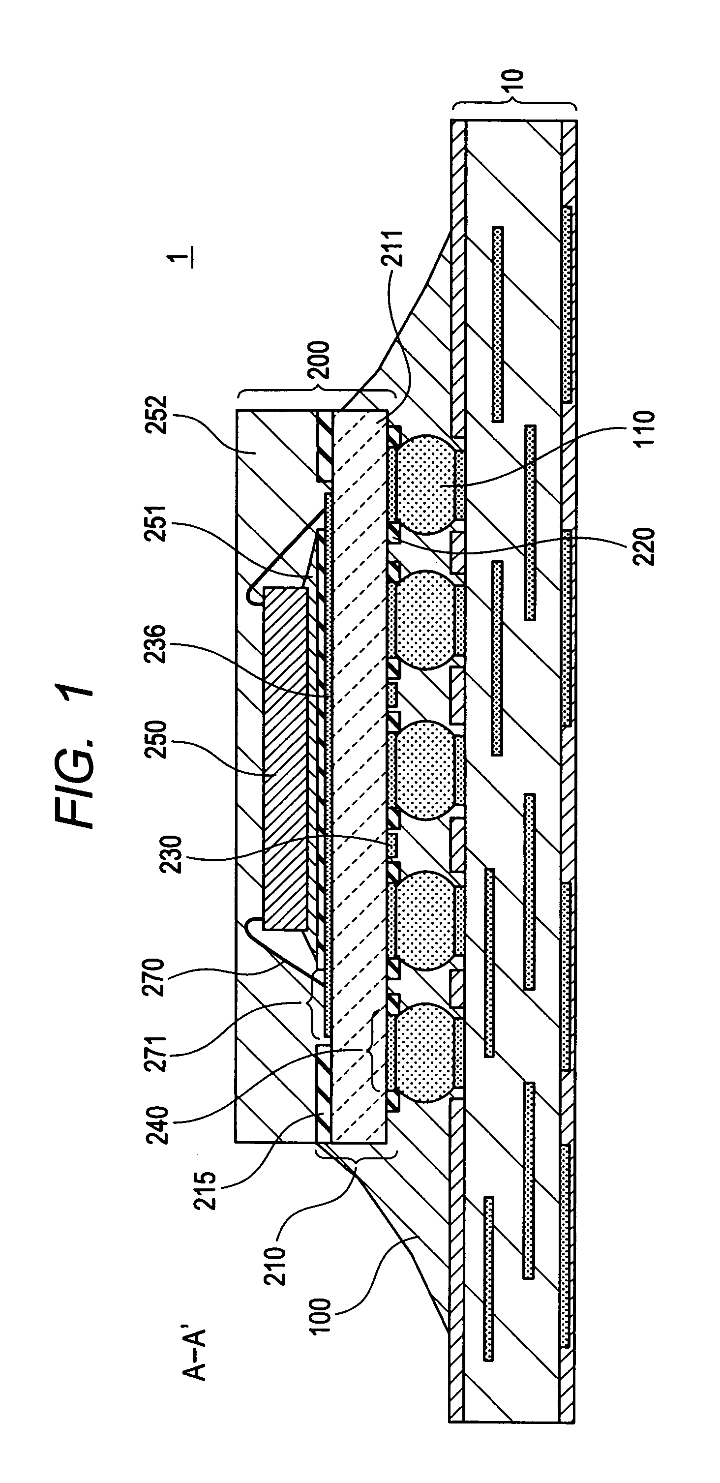
[0026]FIG. 1 is a sectional view showing the structure of a semiconductor device 1 according to the invention. The semiconductor device 1 includes an interconnection substrate 10, a semiconductor package 200, and an underfill resin layer 100. The semiconductor package 200 includes a semiconductor chip 250 and an interposer 210. The interposer 210 has the semiconductor chip 250 mounted over one surface thereof and a plurality of external coupling terminals 240 and an interconnect wire 230 formed over the other surface and is covered by a solder resist layer 220. The semiconductor package 200 is mounted over the interconnection substrate 10, for example, through solder balls 110. The underfill resin layer 100 seals the space between the semiconductor package 200 and interconnection substrate 10. In an area where the interconnect wire 230 passing between two neighboring external coupling terminals 240 intersects with a line connecting the centers of the neighboring external coupling te...
second embodiment
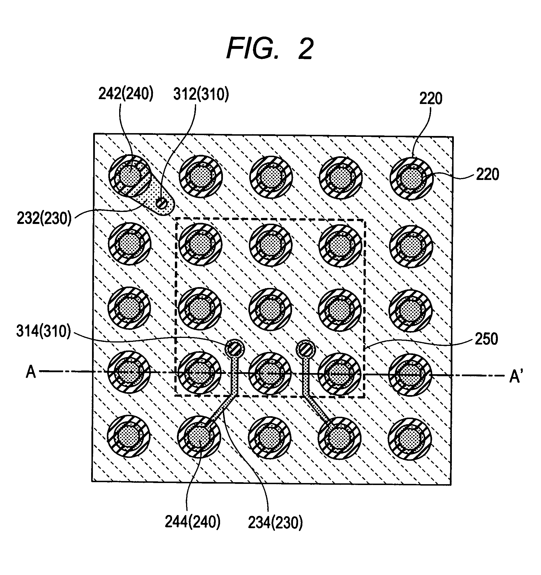
[0037]As shown in FIG. 5, in the interposer 210 a solder resist layer 220 is formed on the interposer 210's surface opposite to the interconnection substrate 10 except the areas of solder resist openings 223 over external coupling terminals 240 and solder resist openings 222. Each solder resist opening 223 lies over an external coupling terminal 240. Each solder resist opening 222 is formed over an interconnect wire 234 between external coupling terminals 240. Each interconnect wire 234 is passed between external coupling terminals 240 arranged along an edge of the semiconductor chip 250.
[0038]Since the semiconductor chip 250 restricts expansion and contraction of the interposer 210, a solder resist crack due to the difference in thermal expansion coefficient tends to occur in an area which overlaps the vicinity of an edge of the semiconductor chip 250. According to the second embodiment, a solder resist opening 222 is provided over an interconnect wire 230 passing between external...
PUM
| Property | Measurement | Unit |
|---|---|---|
| area | aaaaa | aaaaa |
| temperature | aaaaa | aaaaa |
| thermal stress | aaaaa | aaaaa |
Abstract
Description
Claims
Application Information


