Methods for manufacturing crystal devices

a technology of crystal devices and manufacturing methods, which is applied in the direction of manufacturing tools, magnetic bodies, and semiconductor/solid-state device details, etc., can solve the problems of reducing affecting the reliability of the device, and the connection(s) between the electrode pattern and the connection electrode(s) may not be sufficient for the desired reliability, etc., to achieve the effect of simple and easy manufacture of the device, reduced item cost, and easy mass production

Inactive Publication Date: 2012-09-11
NIHON DEMPA KOGYO CO LTD
View PDF13 Cites 3 Cited by
  • Summary
  • Abstract
  • Description
  • Claims
  • Application Information

AI Technical Summary

Benefits of technology

[0010]In some embodiments the crystal lid has a first concavity in its inner main surface and the package base has a second concavity in its inner main surface. These inner surfaces face each other in the finished device, wherein the crystal vibrating piece is situated between the first and second concavities. This configuration allows appropriate oscillation of the crystal vibrating piece to occur without having to adjust the thickness of the crystal vibrating piece.
[0011]Each of the electrodes of the electrode pattern and each connection electrode desirably have a two-metal-layer construction comprising a first metal layer (as a sublayer) and a second metal layer formed on the first metal layer. In the finished device, the second metal layer of the electrode pattern and the second metal layer of the connection electrode(s) are connected together. In devices having such electrode configurations, the respective metals on the crystal frame and on the package base can diffuse together well during the heat and pressure conditions experienced during siloxane bonding.
[0012]An embodiment of a method for manufacturing a crystal device configured as summarized above includes the step of forming a crystal frame and the step of forming a package base, both of crystal material. The method includes the step of forming, either on the second main surface of the crystal frame or on the inner main surface of the package base, at least one step portion. Each step portion has a designated height and is situated to serve as a respective electrode-connection site. On each of the first and second main surfaces of the crystal vibrating piece are formed respective electrodes of the electrode pattern, such as excitation and extraction electrodes. Each extraction electrode extends to the outer frame. On the inner main surface of the package base is formed a respective connection electrode for each extraction electrode. One of the following two situations are utilized in the method: (a) each step portion is located on the second main surface of the crystal frame on which a respective connection electrode extends onto the respective step portion, for connection to the respective connection electrode, or (b) each step portion is located on the inner main surface of the package base on which a respective connection electrode extends onto the respective step portion, for connection to the respective extraction electrode. Each step portion has a height that is less than the thickness of the respective extraction electrode plus the thickness of the respective connection electrode. The step portion can be a simple “step” or a more complex step, the latter including, for example, a comb-like shape or a wave-like shape. Comb-like or wave-like shapes are especially effective for forming reliable and durable connections between electrodes during siloxane bonding.
[0014]These methods allow high productivity of high-reliability crystal devices. High productivity is obtained by forming multiple devices on wafer sandwiches. Also, since the respective coefficients of thermal expansion of all three wafers are substantially equal, siloxane bonding can be conducted easily after aligning the wafers.
[0016]Since the lids and package bases of the crystal devices are made of crystal material (as is the crystal frames), manufacture of the devices is simple and easy. Also, since the electrodes are all bonded together at the same time, mass production is easily achieved, with concomitant reductions in item cost.

Problems solved by technology

During anodic bonding, the Al film unfortunately may exhibit peeling, which reduces the reliability of the device.
Furthermore, conventional crystal units are typically manufactured individually by layering a glass lid and a package base together piece-by-piece, which makes mass production very difficult.
If the gap is less than 10% of the summed thicknesses of the electrode pattern and of the connection electrode, it is still possible to bond together the frame and base, but the resulting connection(s) between the electrode pattern and the connection electrode(s) may not be sufficient for desired reliability.
On the other hand, if the gap is equal to or greater than 30% of the summed thicknesses of the electrode pattern and connection electrode, then the bond between the crystal frame and package base may be insufficient for desired device reliability, regardless of the quality of the connection between the connection electrode(s) and electrode pattern.
Nevertheless, since thermally induced cracking and / or peeling is greatly inhibited by using materials having similar or identical coefficients of thermal expansion, the devices exhibit greater reliability than conventional devices.

Method used


Image

  • Methods for manufacturing crystal devices
  • Methods for manufacturing crystal devices
  • Methods for manufacturing crystal devices

Examples


first embodiment

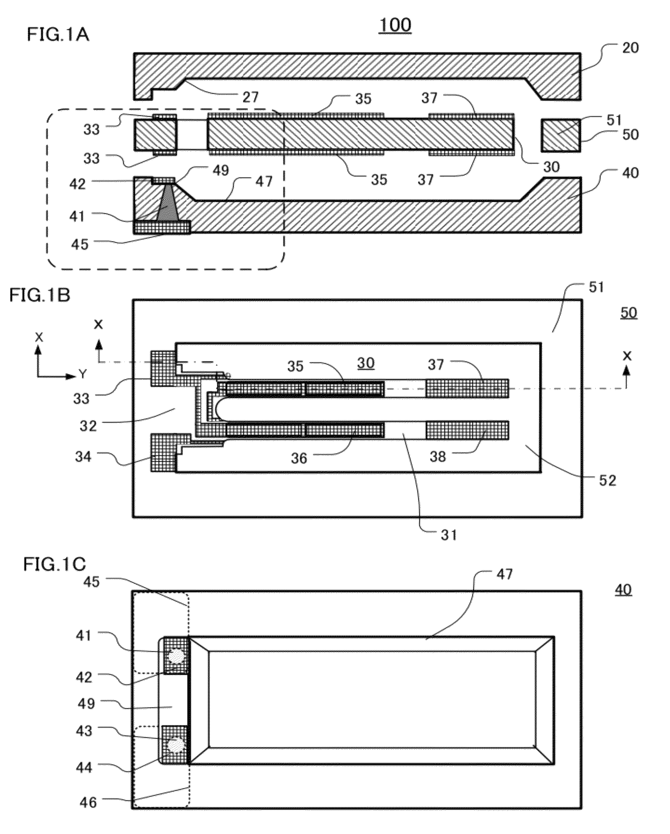
of Method for Bonding Crystal Parts and Electrodes

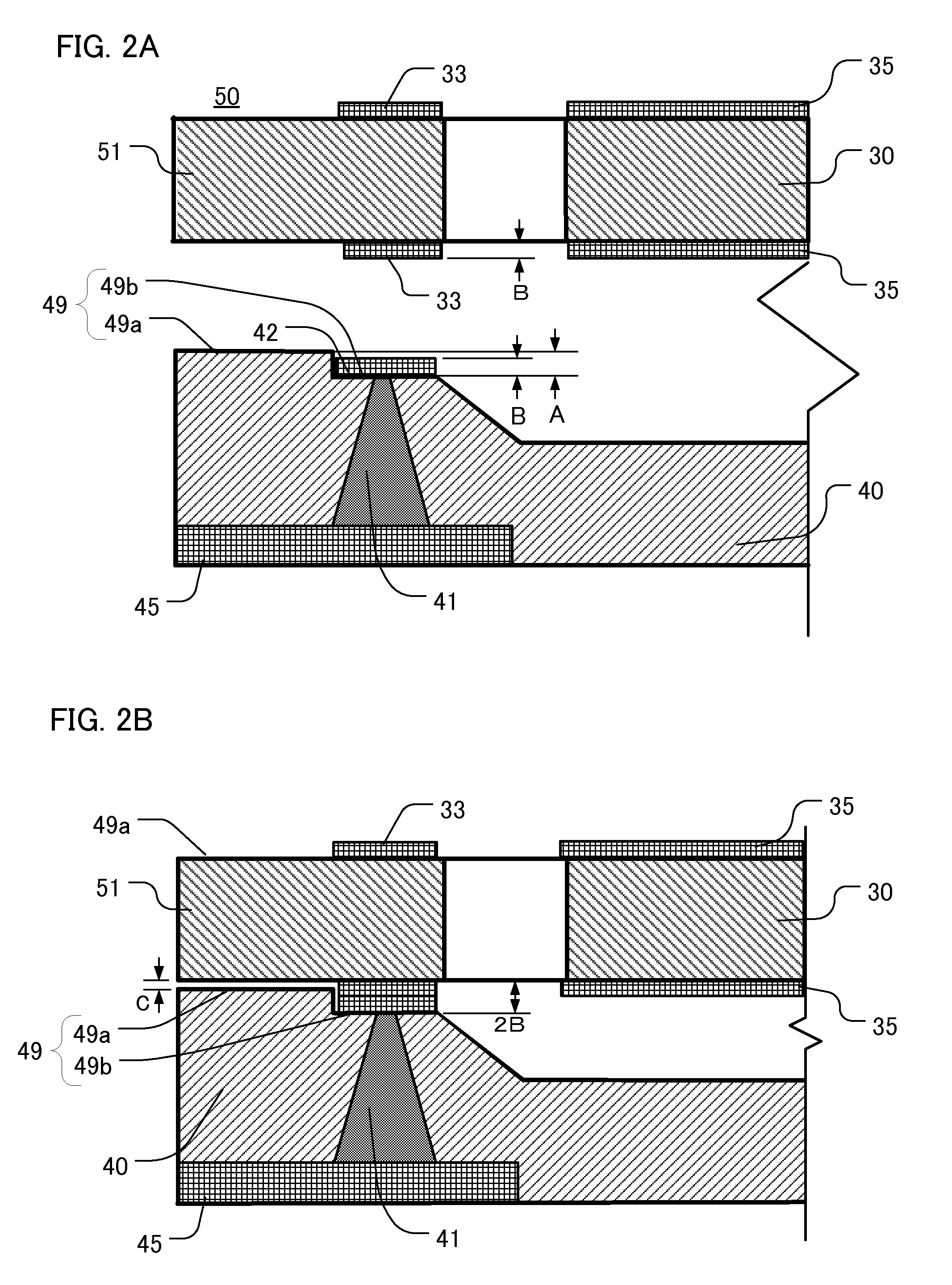
[0040]FIGS. 2A and 2B are enlarged elevational sections of the crystal frame 50 and package base 40 of the first embodiment. FIG. 2A shows the crystal frame 50 and package base 40 vertically separated from each other. FIG. 2B shows a corresponding portion of the crystal frame 50 layered onto the package base 40, but not yet bonded together by siloxane bonding.

[0041]In FIGS. 2A and 2B, at locations where the first connecting electrode 42 and the second connecting electrode 44 (see FIG. 1C) are formed on the package base 40, a respective step portion 49 is formed. See FIG. 2G, which shows two step portions 49A, 49B. Each step portion 49A, 49B includes a respective first step 49a and a respective second step 49b. The second step 49b is formed by wet etching and has a depth of 2500 Å to 3000 Å relative to the first step 49a. The thickness B of each of the first extraction electrode 33 and of the second extraction electrode 34 (not illust...

second embodiment

[0045]FIG. 2C is an enlarged elevational section of the crystal frame 50 and package base 40 of a second embodiment. On the lower surface of the crystal frame 50, a step portion 59 (configured as a depression and including a first step 59a and a second step 59b), is situated where the first extraction electrode 33 and second extraction electrode 34 (see FIG. 1C) are formed. The first step 59a is a respective portion of the lower main surface of the crystal frame (FIG. 2C). The depth A of the second step 59b relative to the first step 59a is 2500 Å to 3000 Å. The thickness B of each of the first and the second electrodes 33, 34, and of plus each of the first and second connection electrodes 42, 44, respectively, is 1500 Å to 2000 Å, so that the total thickness of each pair of these electrodes (33, 42 and 34, 44) is 3000 Å to 4000 Å. The difference between the total thickness (2×B) of a pair of electrodes and the depth A of the step portion 59 is a space C (FIG. 2B) having a thickness...

third embodiment

[0046]FIG. 2D is an enlarged elevational section of a portion of the crystal frame 50 and package base 40 of a third embodiment. On the lower surface of the crystal frame 50 stepped projections 59′ are formed (only one is shown). Each stepped projection 59′ includes a respective first step 59′a and a respective second step 59′b. Each stepped projection 59′ is formed where the first extraction electrode 33 and second extraction electrode 34 (see FIG. 1C), respectively, are formed. The height A of the second step 59′b relative to the height of the lower main surface of the crystal frame 50 (i.e., the first step 59′a) is 2500 Å to 3000 Å. The total thickness of an extraction electrode and corresponding connection electrode is 3000 Å to 4000 Å. The difference in total electrode thickness (2×B) and the depth A is a space C having a height of 500 Å to 1000 Å. By maintaining the thickness of the space C in this manner, the first and second extraction electrodes 33, 34, are reliably connect...


PUM

PropertyMeasurementUnit
temperatureaaaaaaaaaa
melting pointaaaaaaaaaa

Abstract

Crystal devices are disclosed, of which an exemplary device includes a crystal frame comprising a crystal vibrating piece having an electrode pattern and an outer frame supporting the crystal vibrating piece. The device also includes a crystal package base including at least one connection electrode formed on a first main surface and at least one external electrode formed on a second main surface, wherein the second main surface is opposite the first main surface. The crystal frame and crystal base are layered together with a lid wafer to form a 3-layer sandwich. The layers of the sandwich are bonded together by siloxane bonding, which results in the connection electrodes contacting the electrode pattern on the crystal vibrating piece.

Description

CROSS REFERENCE TO RELATED APPLICATIONS[0001]This is the U.S. National Stage of International Application No. PCT / JP2008 / 001751, filed Jul. 3, 2008, which claims priority to and the benefit of JP 2007-227344, filed Sep. 3, 2007, both of which are being incorporated herein by reference in their respective entireties.FIELD[0002]This disclosure pertains to, inter alia, crystal devices made entirely of crystal material, each device including a lid and a package base that form a respective package around a crystal vibrating piece, and to methods for manufacturing same.DESCRIPTION OF THE RELATED ART[0003]With the progress of miniaturization and / or increases in the operating frequency of mobile communication apparatus and office automation (OA) equipment, crystal devices used in this equipment must be progressively smaller and / or operate at higher frequency. A conventional crystal device is formed by layering a lid material and a package material comprising glass or ceramic and sealing by ...

Claims


Application Information

Patent Timeline
Patent Type & Authority Patents(United States)
IPC IPC(8): H04R31/00
CPCH03H9/0595H03H9/1035H03H9/215H01L23/10H01L2924/0002Y10T16/381Y10T29/42Y10T16/126Y10T29/49005Y10T29/4908Y10T16/585H01L2924/00
Inventor INOSE, NAOTOTAKEUCHI, TOSHIAKI
Owner NIHON DEMPA KOGYO CO LTD
Why Eureka
Try Eureka