

Analog-to-digital converter, analog-to-digital converting method, solid-state image pickup device, and camera system
an analog-to-digital converter and digital converter technology, applied in the field of analog-to-digital converters, solid-state image pickup devices, camera systems, etc., can solve the problems of difficult to improve the precision of ad conversion, adc becomes outside the ad range (overflow), and the offset voltage generated is difficult to be determined. , to achieve the effect of high precision, improved conversion processing speed and extended dynamic rang
- Summary
- Abstract
- Description
- Claims
- Application Information
AI Technical Summary
Benefits of technology
Problems solved by technology
Method used
Image

Examples
first embodiment
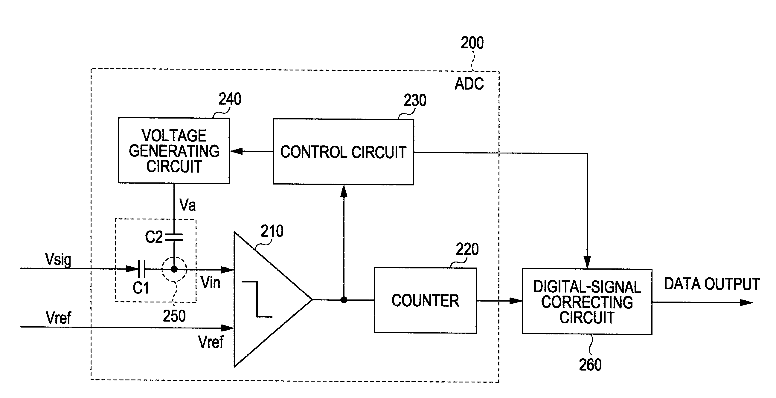
[0092]FIG. 4 is a block diagram showing an exemplary structure of an ADC according to a first embodiment.
[0093]Referring to FIG. 4, the ADC 200 is shown. Also, the comparator 151 shown in FIG. 3 is denoted by reference numeral 210.
[0094]The ADC 200 shown in FIG. 4 includes the comparator 210 (151), a counter 220 that counts a comparison time of the comparator 210, a control circuit 230 that monitors an output of the comparator 210, a voltage generating circuit 240 that generates a DC voltage in accordance with the monitoring result obtained by the control circuit 230, a capacitor C1 connected to an analog-signal (Vsig) input terminal of the comparator 210, a capacitor C2 connected to an output side of the voltage generating circuit 240, an analog adder 250 that adds an analog signal Vsig via the capacitor C1 and a DC signal via the capacitor C2, and a digital-signal correcting circuit 260.
[0095]In the structure shown in FIG. 4, the analog adder 250 is a wired-OR gate.
[0096]The compa...
second embodiment
[0162]FIG. 9 is a block diagram showing an exemplary structure of an ADC according to a second embodiment.
[0163]An ADC 200C according to the second embodiment includes, besides the structure of the ADC 200 according to the first embodiment, which is shown in FIG. 4, a memory 270 whose initial value can be set. In accordance with a signal S230 from the control circuit 230, different initial values of the counter 220 can be selected.
[0164]FIG. 10 is a timing chart for illustrating the operation of the ADC shown in FIG. 9.
[0165]Hereinafter, the operation of the ADC shown in FIG. 9 will be described with reference to FIG. 10.
Operation
[0166]In a period A, a signal voltage Vsig, a voltage Va from the voltage generating circuit 240, and a reference wave Vref are set to fixed voltages. An output of the comparator 210 is determined by the control circuit 230, and the output voltage Va of the voltage generating circuit 240 is switched.
[0167]When the output of the comparator 210 is 0 V, the co...
third embodiment
[0210]FIG. 15 is a block diagram showing an exemplary structure of column-ADCs according to a third embodiment.
[0211]Column-ADCs according to the third embodiment each include, on a column-by-column basis, a counter 220E whose initial value can be set, and a memory 270E. In accordance with a signal from a control circuit 230E, different initial values of the counter 220E can be selected. The arrayed structure includes a common reference signal Vref and a common voltage generating source 290.
[0212]Referring to FIG. 15, the voltage generating source 290 is common to all columns and is arranged outside the column-ADCs. Since there is only one voltage generating source 290, the circuit dimensions are not much increased.
[0213]As a modification of the foregoing structure, a counter-initial-value memory may be shared by all columns, and the initial value of each counter 220E may be selected by a corresponding one of the control circuits 230E.
[0214]Alternatively, the structure may include a...
PUM
 Abstract
Description
Claims
Application Information