Selective epitaxial formation of semiconductor films

a technology of epitaxial formation and semiconductor, applied in the direction of basic electric elements, electrical equipment, semiconductor devices, etc., can solve the problems of non-substitutional doping and complex substitutional doping in the pla

Active Publication Date: 2012-10-02
ASM IP HLDG BV
View PDF272 Cites 450 Cited by
  • Summary
  • Abstract
  • Description
  • Claims
  • Application Information

AI Technical Summary

Problems solved by technology

However, in practice in situ substitutional doping is complicated by the tendency for the dopant to incorporate non-substitutionally during deposition, for example, by incorporating interstitially in domains or clusters within the silicon, rather than by substituting for silicon atoms in the lattice structure.
Non-substitutional doping complicates, for example, carbon doping of silicon, carbon doping of silicon germanium, and doping of silicon and silicon germanium with electrically active dopants.

Method used


Image

  • Selective epitaxial formation of semiconductor films
  • Selective epitaxial formation of semiconductor films
  • Selective epitaxial formation of semiconductor films

Examples


Embodiment Construction

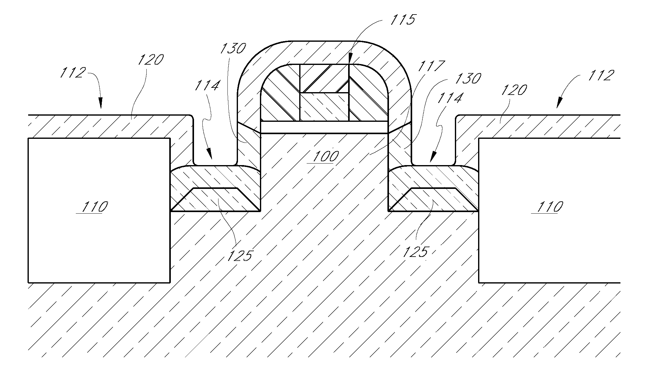
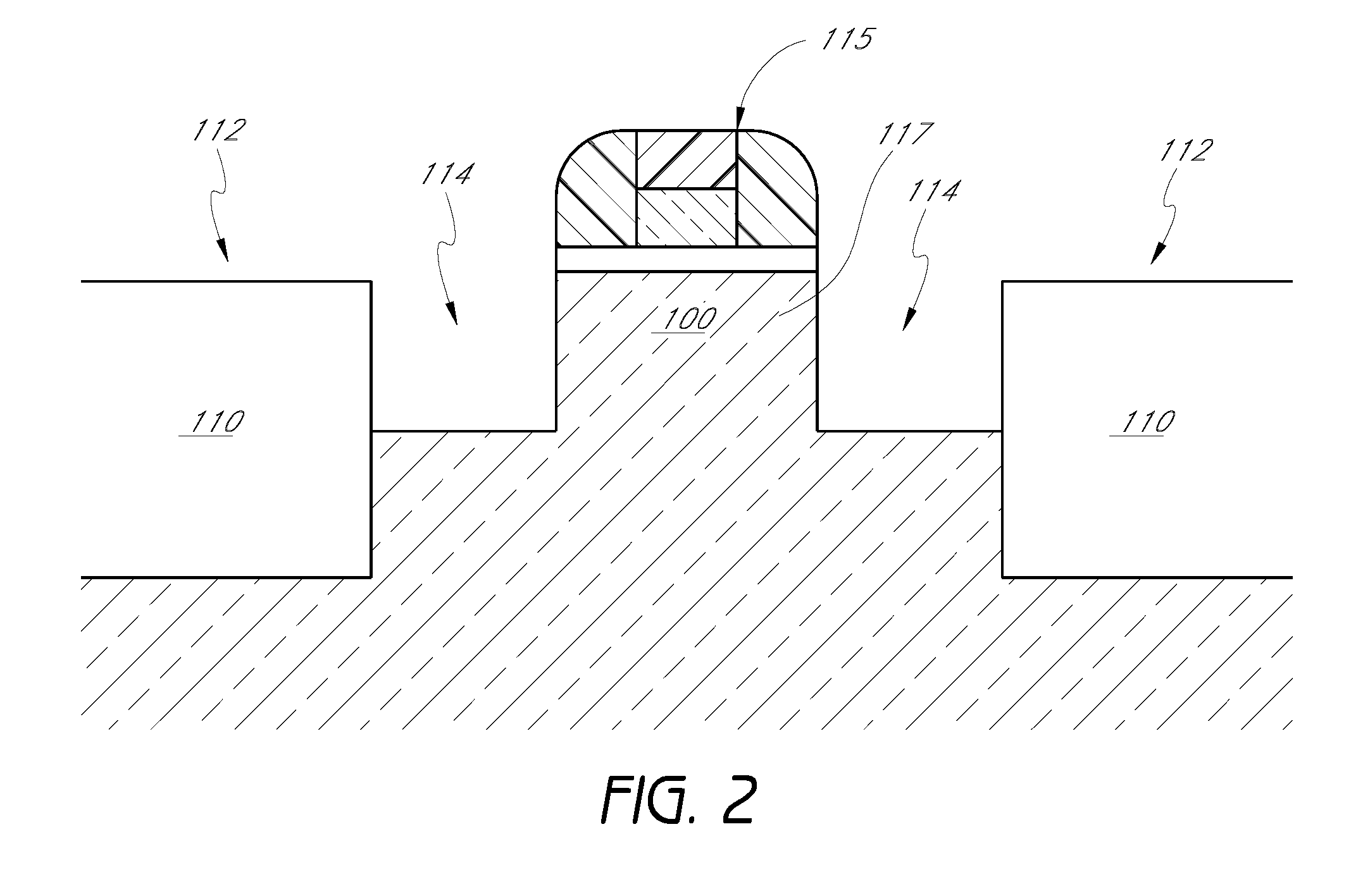
[0032]Deposition techniques often attempt to tailor the amount or kind of deposition in different regions of a substrate. For example, U.S. Pat. No. 6,998,305 recognizes that simultaneous etch and deposition reactions are know for selective deposition on silicon without depositing on silicon oxide. To control deposition on a third type of surface, namely an exposed transistor gate, the '305 patent teaches cyclically alternating a selective deposition with an etch phase. However, the inventors have recognized that selective deposition chemistries sometimes have undesirably effects on the deposited layers. While the described embodiments involve the specific example of carbon-doped silicon for NMOS applications, the skilled artisan will appreciate that the methods described herein have application to a variety of semiconductor applications where selective formation of a layer is desired but etchants can interfere with desired properties of the deposited layer.

[0033]Deposition methods ...


PUM

PropertyMeasurementUnit
band gapaaaaaaaaaa
deposition temperatureaaaaaaaaaa

Abstract

Epitaxial layers are selectively formed in semiconductor windows by a cyclical process of repeated blanket deposition and selective etching. The blanket deposition phases leave non-epitaxial material over insulating regions, such as field oxide, and the selective etch phases preferentially remove non-epitaxial material while deposited epitaxial material builds up cycle-by-cycle. Quality of the epitaxial material improves relative to selective processes where no deposition occurs on insulators. Use of a germanium catalyst during the etch phases of the process aid etch rates and facilitate economical maintenance of isothermal and / or isobaric conditions throughout the cycles. Throughput and quality are improved by use of trisilane, formation of amorphous material over the insulating regions and minimizing the thickness ratio of amorphous:epitaxial material in each deposition phase.

Description

CROSS-REFERENCE TO RELATED APPLICATIONS[0001]This application claims the priority benefit under 35 U.S.C. §119(e) to U.S. provisional application No. 60 / 811,703, filed Jun. 7, 2006.[0002]This application is also related to U.S. patent application Ser. No. 11 / 343,275 (filed 30 Jan. 2006), U.S. patent application Ser. No. 11 / 343,264 (filed 30 Jan. 2006), U.S. Patent Application Publication 2003 / 0036268 (filed 29 May 2002), and U.S. Pat. No. 6,998,305 (filed 23 Jan. 2004). The entire disclosure of all of these related applications is hereby incorporated by reference herein.FIELD OF THE INVENTION[0003]This invention relates generally to the deposition of silicon-containing materials in semiconductor processing, and relates more specifically to selective formation of silicon-containing materials on semiconductor windows.BACKGROUND OF THE INVENTION[0004]In forming integrated circuits, epitaxial layers are often desired in selected locations, such as active area mesas among field isolation...

Claims


Application Information

Patent Timeline
Patent Type & Authority Patents(United States)
IPC IPC(8): H01L21/336
CPCH01L21/02529H01L21/02532H01L21/02576H01L21/02636H01L29/7848H01L29/66628H01L29/66636H01L29/78H01L29/1608H01L29/165
Inventor BAUER, MATTHIASWEEKS, KEITH DORAN
Owner ASM IP HLDG BV
Why Eureka
Try Eureka