Light-emitting element

a technology of light-emitting elements and substrates, which is applied in the direction of discharge tubes/lamp details, discharge tubes/lamp details, incadescent envelopes/vessels, etc., can solve the problems of reducing the light-emitting efficiency, affecting the reliability of the sensor, and difficult to completely reflect primary light, so as to reduce the peak intensity of light, suppress the excitation of the substrate, and reduce the light energy arriving at the substrate

Active Publication Date: 2012-10-02
DOWA ELECTRONICS MATERIALS CO LTD
View PDF18 Cites 0 Cited by
  • Summary
  • Abstract
  • Description
  • Claims
  • Application Information

AI Technical Summary

Benefits of technology

[0012]A light-emitting element according to the present invention includes a light dispersing multilayered film disposed between a substrate and a reflective film and formed by two or more types of light dispersing layers, and the light dispersing multilayered film multiple-disperses a secondary light excited by a primary light passing through the reflective film into plural wavelengths, and discharges the secondary light. More specifically, energy of the primary light passing through the reflective film is divided into plural wavelengths, so that excitement and discharge are performed little by little; this reduces the light energy arriving at the substrate, thereby suppressing excitation of the substrate; and, a peak intensity of the light is reduced, whereby the deleterious effect on the reliability of operation of a sensor is reduced. Further, the peak intensity is reduced without absorbing the excited light, thereby preventing heat from being generated within the light-emitting element. Accordingly, it is possible to provide a light-emitting element possessing the improved reliability.

Problems solved by technology

The primary light directing toward a rear surface of the light-emitting element is absorbed or scattered by a rear-surface electrode or a substrate, and hence does not contribute directly to a light output, which causes the reduction of a light-emitting efficiency.
However, with this technique, it is difficult to completely reflect the primary light, that is, part of the primary light passes through the reflective film and reaches the substrate, and an excited light is secondarily emitted from the substrate.
This excited light from the substrate has a wavelength different from the primary light, and hence, causes a problem that the excited light serves as a noise when used in a sensor for example, possibly having a deleterious effect on reliability of operation of the sensor.
Further, in a case of suppressing the excited light from the substrate by absorbing the light, the excited light is accumulated as heat within the light-emitting element, which also has a deleterious effect on the reliability of operation of the sensor.
The purposes of these disclosed techniques are to control or suppress the intensity of the generated exited light, but a peak intensity of the excited light generated at the substrate cannot be sufficiently suppressed.
Further, in the case of this method of controlling the excited light, light energy is absorbed, so that heat is accumulated.

Method used


Image

  • Light-emitting element
  • Light-emitting element
  • Light-emitting element

Examples


example 1

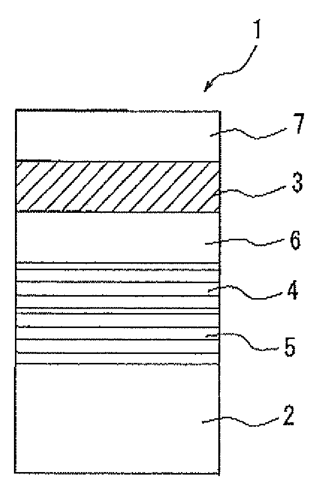
[0041]By using the MOCVD method, a light-emitting element (total thickness (excluding a substrate): 3.9 μm) according to the present invention was formed by sequentially growing: a light dispersing multilayered film (831.5 nm, dopant Se); an n-reflective film (thickness: 1.8 μm, layer formed by repeating Al0.45Ga0.55As (42.3 nm) / AlAs (47.3 nm) 20 times, dopant Se); an n-clad layer (thickness: 90 nm, Al0.5In0.5P, dopant Se); a light-emitting layer (thickness: 84 nm, InyGa(1-y)P (y=0.53), undoped); a p-clad layer (thickness: 180 nm, Al0.5In0.5P, dopant Mg); and, a p-reflective layer (thickness: 0.9 μm, layer formed by repeating Al0.45Ga0.55As (42.3 nm) / AlAs (47.3 nm) 10 times, dopant C) on the GaAs substrate (Si doped, plane direction: (100) 15° off, thickness: 350 μm). The p-reflective layer functioned as a vertical resonator with an n-reflective layer, and was inserted to narrow the emission spectrum and make the light-emitting element further suitable for use in sensors.

[0042]The l...

example 2

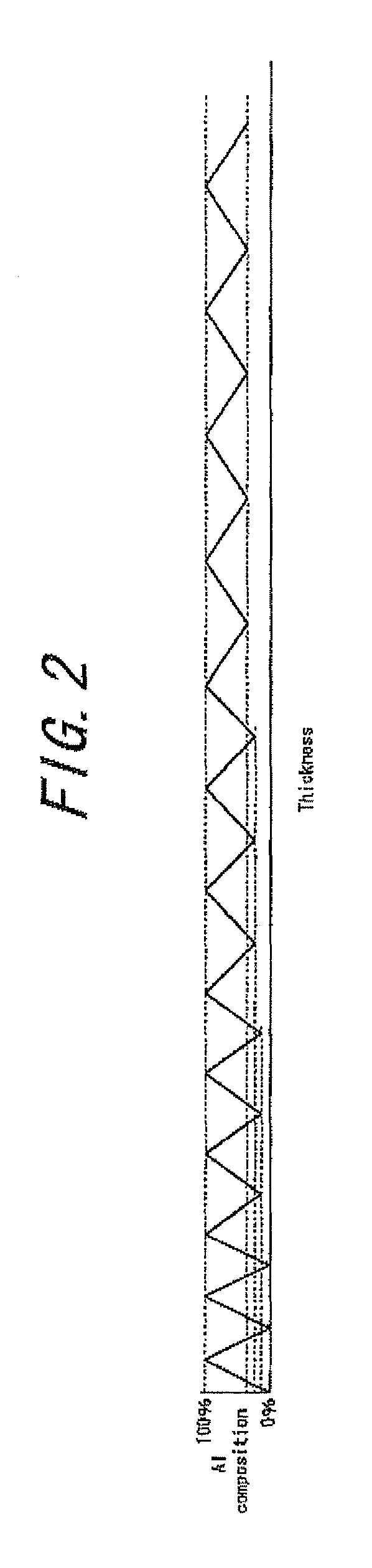
[0045]A light-emitting element similar to that in Example 1 was prepared, except that the light dispersing multilayered film in Example 2 was made of a AlxGa(1-x)As material (0≦x≦1), and, as illustrated in FIG. 4, the Al composition in the AlxGa(1-x)As material was designed such that the lower Al composition was formed by 0%×2, 10%×, 15%×2, 20%×2, 25%×3, 30%×4, and 35%×5 cycles, and the thicknesses of the respective sets of cycles were set at 65.9 nm, 67.8 nm, 68.8 nm, 69.8 nm, 70.7 nm, 71.7 nm, and 72.7 nm so as to reflect the wavelength of 870 nm of the substrate excited light. Note that, since the cycle of the lower Al composition 0% to the higher Al composition 100% (32.9 nm) on the left end and the cycle of the higher Al composition 100% to the lower Al composition 35% (36.4 nm) on the right end do not have the confining effect, these cycles are not included in the number of pairs.

[0046]In addition, a PL measurement was made on a sample having only the light dispersing multilay...


PUM


Abstract

A light-emitting element comprising a substrate; a light-emitting layer disposed above the substrate and emitting a primary light; and, a reflective film disposed between the substrate and the light-emitting layer and formed by at least one layer that reflects the primary light, in which the light-emitting element further comprises a light dispersing multilayered film disposed between the substrate and the reflective film and formed by two or more types of light dispersing layers, and the light dispersing multilayered film multiple-disperses a secondary light into plural wavelengths and discharges the secondary light, which is excited by the primary light passing through the reflective film.

Description

TECHNICAL FIELD[0001]The present invention relates to a light-emitting element that emits a primary light at a light-emitting layer, and, in particular, to a light-emitting element used, for example, for sensors and the like.BACKGROUND ART[0002]In general, in a light-emitting element having a double hetero structure, a primary light emitted at a light-emitting layer directs not only toward a front surface of the light-emitting element but also isotropically toward all directions. The primary light directing toward a rear surface of the light-emitting element is absorbed or scattered by a rear-surface electrode or a substrate, and hence does not contribute directly to a light output, which causes the reduction of a light-emitting efficiency.[0003]In order to suppress such a phenomenon as this, there has been developed a technique in which a reflective film formed by at least one layer and reflecting the primary light is arranged between the substrate and the light-emitting layer. How...

Claims


Application Information

Patent Timeline
Patent Type & Authority Patents(United States)
IPC IPC(8): H05B33/00
CPCH01L33/10H01L33/08
Inventor IWATA, MASATOSHITASAKI, NORIOKOBAYASHI, YOSHIYUKIMATSUURA, TETSUYA
Owner DOWA ELECTRONICS MATERIALS CO LTD
Why Eureka
Try Eureka