Semiconductor device including a die region designed for aluminum-free solder bump connection and a test structure designed for aluminum-free wire bonding

a technology of aluminum-free solder bump connection and semiconductor device, which is applied in the direction of individual semiconductor device testing, semiconductor/solid-state device testing/measurement, instruments, etc., can solve the problems of difficult to remove the metal mask after the deposition process without damaging the solder pads, difficult to achieve copper bond pads, and more complex process flow. achieve the effect of avoiding highly complex deposition and patterning process, avoiding aluminum-based process steps, and high efficiency

Active Publication Date: 2012-10-09
ADVANCED MICRO DEVICES INC
View PDF14 Cites 4 Cited by
  • Summary
  • Abstract
  • Description
  • Claims
  • Application Information

AI Technical Summary

Benefits of technology

[0018]Generally, the subject matter disclosed herein relates to a technique and respective semiconductor devices in which a bump structure is formed in device regions on the basis of a copper-based metal region, thereby avoiding highly complex deposition and patterning processes for forming barrier / adhesion layers and aluminum material, while also providing the possibility of enabling wire bonding in respective test regions and avoiding aluminum-based process steps. Moreover, the subject matter disclosed herein provides substantially similar final passivation layer stacks in test regions and actual device regions which, in some illustrative aspects, may be accomplished in the same substrates when substrates are contemplated that are dedicated for reliability tests. Consequently, the present disclosure enables the highly efficient process technique for forming bump structures in device regions and wire bonding structures in test regions without requiring aluminum-based techniques, thereby freeing resources in terms of equipment and clean room areas that would otherwise be required for the aluminum technology, while nevertheless providing the advantages associated with the wire bonding of respective test structures.

Problems solved by technology

Moreover, it is extremely difficult to remove the metal mask after completion of the deposition process without damaging the solder pads, particularly when large wafers are processed or the pitch between adjacent solder pads decreases.
The complexity of advanced semiconductor devices, such as CPUs and the like, typically requires the provision of specifically designed test structures for estimating the quality and thus reliability of the manufacturing flow and the materials used.
Similarly, many back end of line processes may require a thorough monitoring, such as the electromigration behavior, or generally stress-induced degradation of sophisticated wiring structures, in particular, as typically increasingly low-k dielectric materials are used in the wiring level in combination with highly conductive metals, such as copper and the like.
On the other hand, since the formation of aluminum-based solder bump structures may result in a more complex process flow compared to approaches for directly forming bump structures on the basis of copper-based contact areas in sophisticated metallization systems provided on the basis of copper, possibly in combination with low-k dielectric materials, great efforts are being made in establishing process techniques for avoiding the usage of aluminum in the back end of line (BEOL) process.
However, a bonding on copper bond pads is very difficult to achieve due to an inhomogeneous self-oxidization of the copper surface in combination with extensive corrosion, which may result in highly non-reliable bond connections.
For this reason, metallization systems including actual die regions and respective test structures may nevertheless be manufactured on the basis of aluminum in an attempt to utilize well-established infrastructure of aluminum-based bump structure techniques in combination with well-approved wire bond processes, thereby however contributing to enhanced process complexity for copper-based metallization systems, as will be described in more detail with reference to FIGS. 1a-1d.

Method used


Image

  • Semiconductor device including a die region designed for aluminum-free solder bump connection and a test structure designed for aluminum-free wire bonding
  • Semiconductor device including a die region designed for aluminum-free solder bump connection and a test structure designed for aluminum-free wire bonding
  • Semiconductor device including a die region designed for aluminum-free solder bump connection and a test structure designed for aluminum-free wire bonding

Examples


Embodiment Construction

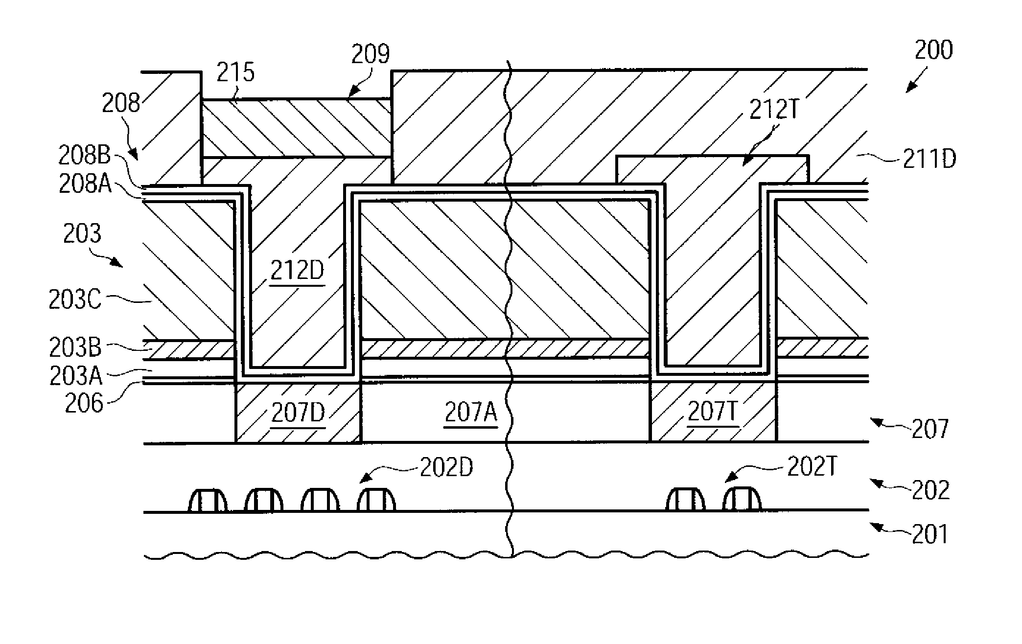
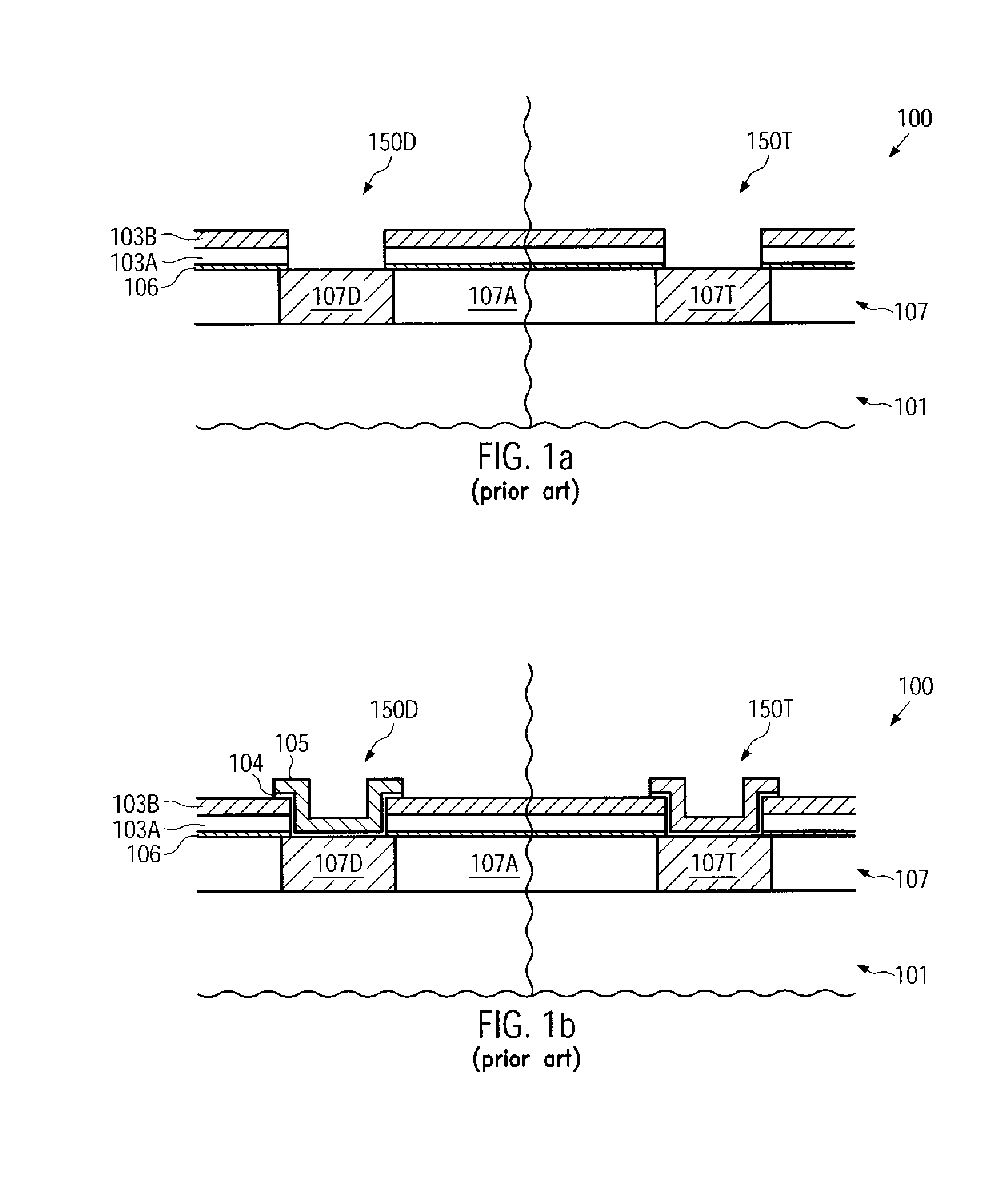
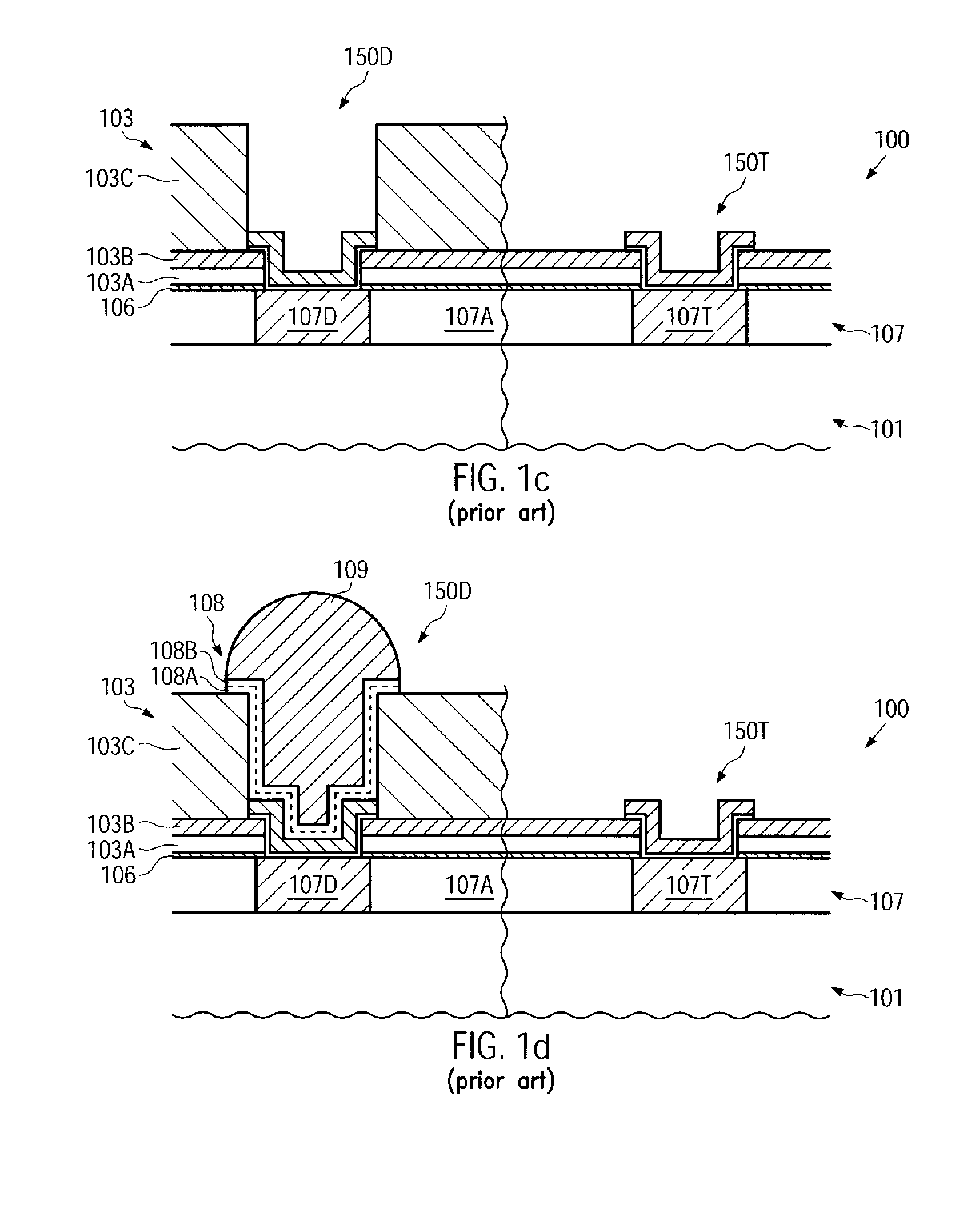
[0031]Various illustrative embodiments of the invention are described below. In the interest of clarity, not all features of an actual implementation are described in this specification. It will of course be appreciated that in the development of any such actual embodiment, numerous implementation-specific decisions must be made to achieve the developers' specific goals, such as compliance with system-related and business-related constraints, which will vary from one implementation to another. Moreover, it will be appreciated that such a development effort might be complex and time-consuming, but would nevertheless be a routine undertaking for those of ordinary skill in the art having the benefit of this disclosure.

[0032]The present subject matter will now be described with reference to the attached figures. Various structures, systems and devices are schematically depicted in the drawings for purposes of explanation only and so as to not obscure the present disclosure with details ...


PUM


Abstract

In sophisticated semiconductor devices including copper-based metallization systems, a substantially aluminum-free bump structure in device regions and a substantially aluminum-free wire bond structure in test regions may be formed on the basis of a manufacturing process resulting in identical final dielectric layer stacks in these device areas. The number of process steps may be reduced by making a decision as to whether a substrate is to become a product substrate or test substrate for estimating the reliability of actual semiconductor devices. For example, nickel contact elements may be formed above copper-based contact areas wherein the nickel may provide a base for wire bonding or forming a bump material thereon.

Description

BACKGROUND OF THE INVENTION[0001]1. Field of the Invention[0002]The present disclosure generally relates to the formation of integrated circuits, and, more particularly, to a back end of line processing for providing a bump structure arranged for direct solder bump connection in a die area while enabling wire bonding of bond pads located outside the die area, such as the frame region of semiconductor devices.[0003]2. Description of the Related Art[0004]In manufacturing integrated circuits, it is usually necessary to package a chip and provide leads and terminals for connecting the chip circuitry with the periphery. In some packaging techniques, chips, chip packages or other appropriate units may be connected by means of solder balls, formed from so-called solder bumps, that are formed on a corresponding layer of at least one of the units, for instance, on a dielectric passivation layer of the microelectronic chip. In order to connect the microelectronic chip with the corresponding c...

Claims


Application Information

Patent Timeline
Patent Type & Authority Patents(United States)
IPC IPC(8): H01L21/44
CPCH01L24/13H01L22/34H01L24/11H01L24/05H01L2924/01013H01L2924/01068H01L2924/01022H01L2924/01028H01L2924/01029H01L2924/01033H01L2924/01047H01L2924/0105H01L2924/01073H01L2924/01074H01L2924/01078H01L2924/01079H01L2924/01082H01L2924/014H01L2924/04941H01L2924/04953H01L2924/05042H01L2924/14H01L2924/19043H01L2924/30105H01L2924/01014H01L2924/01019H01L2924/01006H01L2924/00013H01L2924/1306H01L2224/0401H01L2924/01075H01L2224/05073H01L2224/05644H01L2224/1308H01L2224/13082H01L2224/13155H01L2224/13184H01L2924/01005H01L2924/01007H01L2924/00014H01L2224/13099H01L2924/00
Inventor LEHR, MATTHIASKUECHENMEISTER, FRANKTHIERBACH, STEFFI
Owner ADVANCED MICRO DEVICES INC
Why Eureka
Try Eureka