Reprocessing method of semiconductor substrate, manufacturing method of reprocessed semiconductor substrate, and manufacturing method of SOI substrate

a manufacturing method and semiconductor technology, applied in semiconductor/solid-state device manufacturing, basic electric elements, electric devices, etc., can solve the problems of insufficient security of reprocessing and bonding substrates, and achieve the effect of reducing the amount of a semiconductor removed in reprocessing treatment of semiconductor substrates, facilitating planarity, and reducing the number of times of reprocessing and use of semiconductor substrates

Inactive Publication Date: 2012-10-16
SEMICON ENERGY LAB CO LTD
View PDF139 Cites 8 Cited by
  • Summary
  • Abstract
  • Description
  • Claims
  • Application Information

AI Technical Summary

Benefits of technology

[0006]When a hydrogen ion implantation separation method is employed as a method for manufacturing an SOI substrate, a plurality of SOI substrates can be manufactured from one bond substrate; therefore, there is an advantage that cost for the bond substrate in manufacturing an SOI substrate can be reduced. This is because, when the bond substrate from which a single crystal silicon layer is separated is subjected to reprocessing treatment, the used bond substrate can be reused for manufacturing another SOI substrate.
[0022]According to an embodiment of the disclosed invention, a damaged semiconductor region can be selectively removed with a non-damaged semiconductor region (or a semiconductor region in which the degree of damage is low) left. Accordingly, the amount of a semiconductor removed in reprocessing treatment of the semiconductor substrate can be sufficiently reduced, and the number of times of reprocessing and use of the semiconductor substrate can be sufficiently secured.
[0024]Further, when a reprocessed semiconductor substrate is manufactured by the above method for reprocessing a semiconductor substrate, the amount of a semiconductor removed in the reprocessing treatment can be sufficiently reduced. Accordingly, cost for manufacturing the reprocessed semiconductor substrate can be reduced.
[0025]Furthermore, when an SOI substrate is manufactured using the above reprocessed semiconductor substrate, cost for manufacturing the SOI substrate can be sufficiently reduced.

Problems solved by technology

This step portion becomes a problem in a stage of reprocessing treatment of the bond substrate.
However, in order to remove the step portion by polishing a surface of the bond substrate with a CMP method so that the reprocessed substrate can be used for manufacturing an SOI substrate again as a bond substrate, a semiconductor layer needs to be removed by approximately 10 μm, and thus the number of times of reprocessing and use of the bond substrate cannot be sufficiently secured.

Method used


Image

  • Reprocessing method of semiconductor substrate, manufacturing method of reprocessed semiconductor substrate, and manufacturing method of SOI substrate
  • Reprocessing method of semiconductor substrate, manufacturing method of reprocessed semiconductor substrate, and manufacturing method of SOI substrate
  • Reprocessing method of semiconductor substrate, manufacturing method of reprocessed semiconductor substrate, and manufacturing method of SOI substrate

Examples


embodiment 1

[0056]In this embodiment, a method for reprocessing a semiconductor substrate will be described with reference to FIGS. 1A to 1D and FIGS. 2A and 2B.

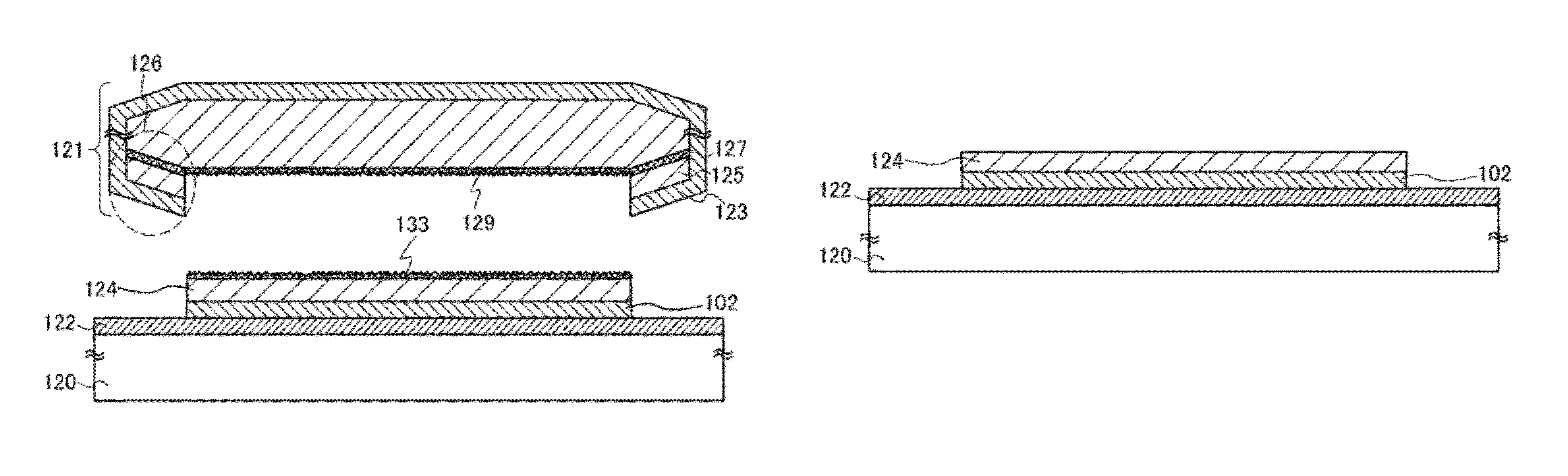
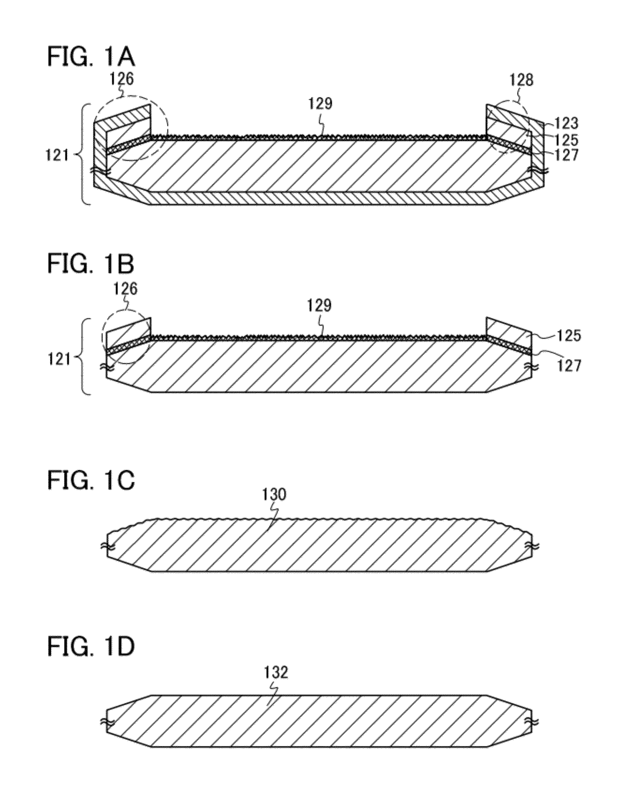
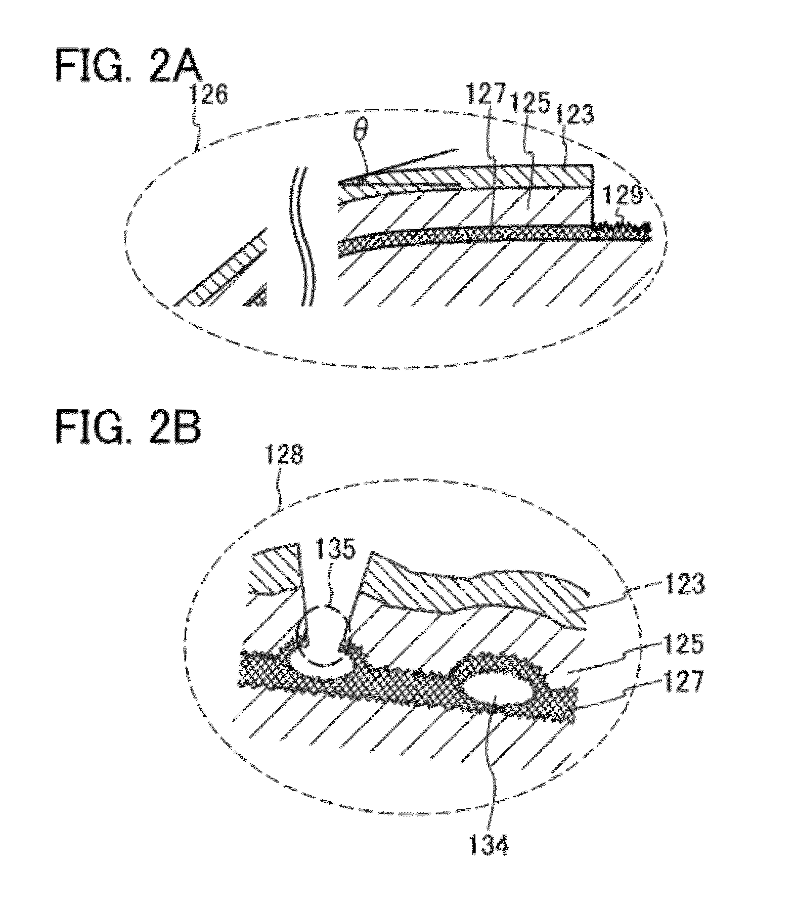
[0057]FIG. 1A illustrates an example of a structure of a semiconductor substrate 121 before reprocessing treatment (a semiconductor substrate from which a semiconductor layer is separated). A step portion 126 exists in a peripheral portion of the semiconductor substrate 121. The step portion 126 includes an insulating layer 123, an unseparated semiconductor region 125, and a semiconductor region 127. Note that both the unseparated semiconductor region 125 and the semiconductor region 127 are damaged and include many crystal defects, voids, blisters, or the like, due to ion irradiation treatment or the like in a manufacturing process of an SOI substrate. In particular, the semiconductor region 127 is a region where damage and embrittlement due to the ion irradiation are remarkable. Therefore, the unseparated semiconductor region 125 and ...

embodiment 2

[0089]In a method for manufacturing an SOI substrate of this embodiment, an SOI substrate is manufactured by bonding a semiconductor layer separated from a semiconductor substrate which is a bond substrate to a base substrate. The semiconductor substrate from which the semiconductor layer has been separated is subjected to reprocessing treatment and reused as a bond substrate. An example of the method for manufacturing an SOI substrate of this embodiment will be described below with reference to FIGS. 2A and 2B, FIGS. 3A to 3C, FIGS. 4A to 4C, FIGS. 5A to 5C, and a manufacturing process chart of an SOI substrate of FIG. 6.

[0090]First, a process of forming an embrittlement region 104 in a semiconductor substrate 100 to prepare for bonding with a base substrate 120 is described. This process relates to treatment for the semiconductor substrate 100 and corresponds to Process A in FIG. 6.

[0091]First, the semiconductor substrate 100 is prepared (see FIG. 3A and the step A-1 in FIG. 6). A...

embodiment 3

[0165]In this embodiment, the case where an SOI substrate is manufactured using a silicon substrate or the like with high heat resistance as a base substrate will be described. Note that a method described in this embodiment is common to the above embodiment in many points. Therefore, different points will be mainly described in this embodiment. Drawings will not be particularly shown in this embodiment because drawings of this embodiment are in common with those of the above embodiment.

[0166]In a semiconductor substrate that is used as a bond substrate, an insulating layer and an embrittlement region are formed. Treatment and the like for the semiconductor substrate, which includes the formation of the insulating layer and the embrittlement region, are similar to those in the above embodiment. Therefore, description in the above embodiment may be referred to for such treatment and the like.

[0167]In this embodiment, a substrate with high heat resistance is used as a base substrate. ...


PUM

PropertyMeasurementUnit
angleaaaaaaaaaa
heightaaaaaaaaaa
distanceaaaaaaaaaa

Abstract

An object of an embodiment of the disclosed invention is to provide a method suitable for reprocessing a semiconductor substrate which is reused to manufacture an SOI substrate. A semiconductor substrate is reprocessed in the following manner: etching treatment is performed on a semiconductor substrate in which a step portion including a damaged semiconductor region and an insulating layer exists in a peripheral portion, whereby the insulating layer is removed; etching treatment is performed on the semiconductor substrate with the use of a mixed solution including a substance that oxidizes a semiconductor material included in the semiconductor substrate, a substance that dissolves the oxidized semiconductor material, and a substance that controls oxidation speed of the semiconductor material and dissolution speed of the oxidized semiconductor material, whereby the damaged semiconductor region is selectively removed with a non-damaged semiconductor region left; and heat treatment under an atmosphere including hydrogen is performed.

Description

TECHNICAL FIELD[0001]One of technical fields of the disclosed invention relates to a method for reprocessing a semiconductor substrate. In addition, the disclosed invention relates to a method for manufacturing a reprocessed semiconductor substrate with the use of the method for reprocessing a semiconductor substrate, and relates to a method for manufacturing an SOI (silicon on insulator) substrate.BACKGROUND ART[0002]In recent years, integrated circuits using an SOI (silicon on insulator) substrate that includes a thin single crystal silicon layer formed on an insulating surface have been developed instead of those using a bulk silicon wafer. The characteristics of the thin single crystal silicon layer formed on the insulating surface make it possible to completely separate transistors formed in the integrated circuit from each other. Further, since fully-depleted transistors can be formed, a semiconductor integrated circuit with high added values such as high integration, high spe...

Claims


Application Information

Patent Timeline
Patent Type & Authority Patents(United States)
IPC IPC(8): H01L21/30
CPCH01L21/02024H01L21/02032H01L21/30604H01L21/324H01L21/3247H01L21/76254H01L21/30608H01L21/84
Inventor OHNUMA, HIDETOHANAOKA, KAZUYA
Owner SEMICON ENERGY LAB CO LTD
Why Eureka
Try Eureka