

Strain-controlled atomic layer epitaxy, quantum wells and superlattices prepared thereby and uses thereof
a strain-controlled, atomic layer technology, applied in the field of semiconductors, can solve the problems of difficult incorporation of nitrogen atoms into gainas quantum wells, poor crystal quality, and difficult industrial processes for high-indium-content dilute-nitride gainasn/gaas structures using metal organic chemical vapor deposition (mocvd)
- Summary
- Abstract
- Description
- Claims
- Application Information
AI Technical Summary
Benefits of technology
Problems solved by technology
Method used
Image

Examples
example 1
Materials and Methods
[0207]InAsN layers were grown on semi-insulating (001)-oriented GaAs substrates using a low-pressure metal organic chemical vapor deposition (MOCVD) upside-down vertical reactor. The grown samples consisted of 1000 Å GaAs buffer layers grown at 650° C., followed by the ALE growth of (Ga)InAs(N) quantum wells at 500° C. capped with a 12 Å layer of GaAs grown conventionally at the same temperature. On top of the nitride layer, 500 Å GaAs spacers were grown at a temperature of 650° C. The low growth temperature of the cap was effected to reduce escape of nitrogen, as discussed hereinbelow.
[0208]The elements which were used in the following examples are listed in the partial periodic table of the elements, presented as Table 1 below.
[0209]
TABLE 1Group IIIGroup VPeriod 2Nitrogen (N)Period 3Period 4Gallium (Ga)Arsenic (As)Period 5Indium (In)Antimony (Sb)
[0210]Trimethylgallium (TMGa) and trimethylindium (TMIn) were used for the ALE growth as Group III sources; arsine (...
example 2
Growth-Rates of Indium Monolayers
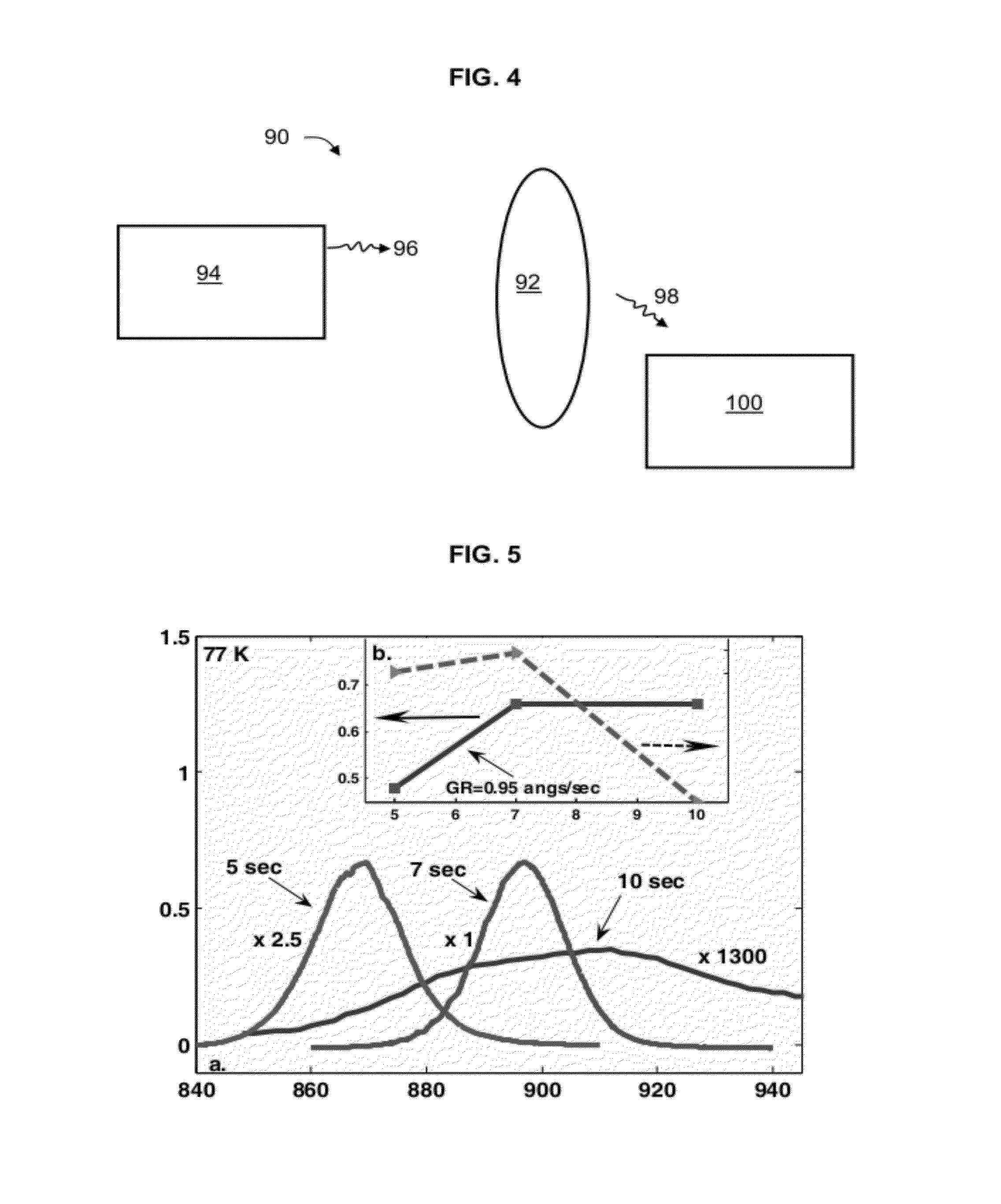
[0213]The time required to grow a single atomic layer (AL) of indium using a constant flow from a TMIn source (“Group III” column) was determined by changing the exposure time of the substrate to the indium source, compared to known time of exposure extracted from conventional growth rates. Three types of samples with quantum wells consisting of two InAs monolayers (ML) growth cycles were prepared with TMIn exposure times of 5, 7, and 10 seconds, followed by a 30 seconds exposure to arsine (AsH3, “Group V” column) to assure full coverage.
[0214]FIGS. 5A-B present the indium monolayer growth as a result of the TMIn exposure times, wherein FIG. 5A presents the PL spectra of the three ALE-grown InAs quantum wells, and FIG. 5B presents the growth rate of the indium arsenide layer as a function of the TMIn exposure time.
[0215]As can be seen in FIG. 5A, the thickness of the InAs layers was found by comparing the calculated energy of the fundamental optical ...
example 3
Incorporation of Nitrogen into InAs Quantum Wells
[0222]The incorporation of nitrogen (N) into the InAs quantum wells was effected by exposing the grown indium atomic layers to a flow of high molar fraction of DMH / H2 without AsH3 for a period of 20 seconds. This high volume of DMH assured full coverage of the atomic layer with N atoms. The red shift of the PL peak between the emissions measured from a reference InAs quantum well without N and the InAsN quantum well, both prepared with the same indium atomic layer sequence, was used to assess the quantity of the N incorporation into the layers. In addition, the results were confirmed from TOF-SIMS measurements of structures containing a few InAsN layers, as described below.
[0223]FIG. 6A shows the PL spectrum of a sample consisting of a two-monolayer InAs quantum well grown using an ALE sequence of [In—As—In—As], and a two-monolayer InAsN quantum well grown using a sequence of [In—N—In—As], where DMH replaced the arsine during the grow...
PUM
 Abstract
Description
Claims
Application Information