Electromagnetic wave oscillating devices

a technology of electromagnetic waves and oscillating devices, applied in the field of electromagnetic wave oscillating devices, can solve the problems of propagation loss, reflection loss, and inability to draw the terahertz wave to the outside, and achieve the effect of preventing incidence and high absorban

Active Publication Date: 2012-11-06
NGK INSULATORS LTD
View PDF10 Cites 13 Cited by
  • Summary
  • Abstract
  • Description
  • Claims
  • Application Information

AI Technical Summary

Benefits of technology

[0060]The following advantageous effects are obtained by providing the film 15 reflecting the electromagnetic wave on the joining surface on the side of the adhesive layer of the supporting body, as exemplified in FIG. 5(b).
[0061]That is, an electrode in not provided on the surface of the oscillating substrate, which provides cut-off state with respect to the generated electromagnetic wave having a wavelength of 0.1 THz to 3 THz. The oscillated electromagnetic wave is thus emitted to the directions of the surface and back face (toward the supporting body) is radiation mode, so that the wave does not reach the side faces of the oscillating substrate.
[0062]It is then proved to be difficult to emit the oscillated electromagnetic wave to the direction of the substrate surface efficiently, since the oscillated electromagnetic wave is scattered without a specific directivity. That is, the terahertz wave having a wavelength of 0.1 THz to 3 THz has a high absorbance by various materials, so that the electromagnetic wave irradiated toward the back face of the oscillating substrate is absorbed by the supporting body and is not emitted to the outside of the device. For example, in the case that the supporting body 13 is made of lithium niobate single crystal, most of the oscillated electromagnetic wave is absorbed by the supporting body having a thickness of as small as about 100 μm. As a result, a considerable portion of the generated electromagnetic wave (about a half) is not emitted to the outside of the device.
[0063]Here, it is found that the electromagnetic wave irradiated in the direction of the back face of the oscillating substrate can be emitted to the outside of the device and the output power can be made two times or more, by forming the film reflecting the electromagnetic wave on the surface of the supporting body on the side of the adhesive layer.
[0064]Besides, if an optical modulator would be operated for the modulation on a frequency band of 0.1 THz to 3 THz, the electromagnetic wave should have been propagated in a supporting body in substrate radiation mode. However, the electromagnetic wave should have been absorbed and disappears so that it is not necessary to provide a film reflecting the electromagnetic wave on the surface of the supporting body.
[0065]According to the present embodiment, the film reflecting the electromagnetic wave refers to a film for (1) preventing the incidence of the electromagnetic wave into the supporting body (Shielding of electromagnetic wave) and (2) irradiating the electromagnetic wave to the side of the oscillating substrate surface (irradiation of electromagnetic wave). The reflectivity of the film reflecting the electromagnetic wave in the air may preferably be 80 percent or higher. The upper limit of the reflectivity is not particularly limited and may be 100 percent.

Problems solved by technology

Further, as the refractive index of the crystal is considerably larger than that of air, it is impossible to draw the terahertz wave to the outside without providing a prism or grating on the crystal surface.
Further, the prism or grating on the crystal surface results in a propagation loss and reflection loss.

Method used


Image

  • Electromagnetic wave oscillating devices
  • Electromagnetic wave oscillating devices
  • Electromagnetic wave oscillating devices

Examples


##ventive example 1

Inventive Example 1

[0068]The terahertz wave oscillating device described referring to FIGS. 3, 4 and 5(a) was produced.

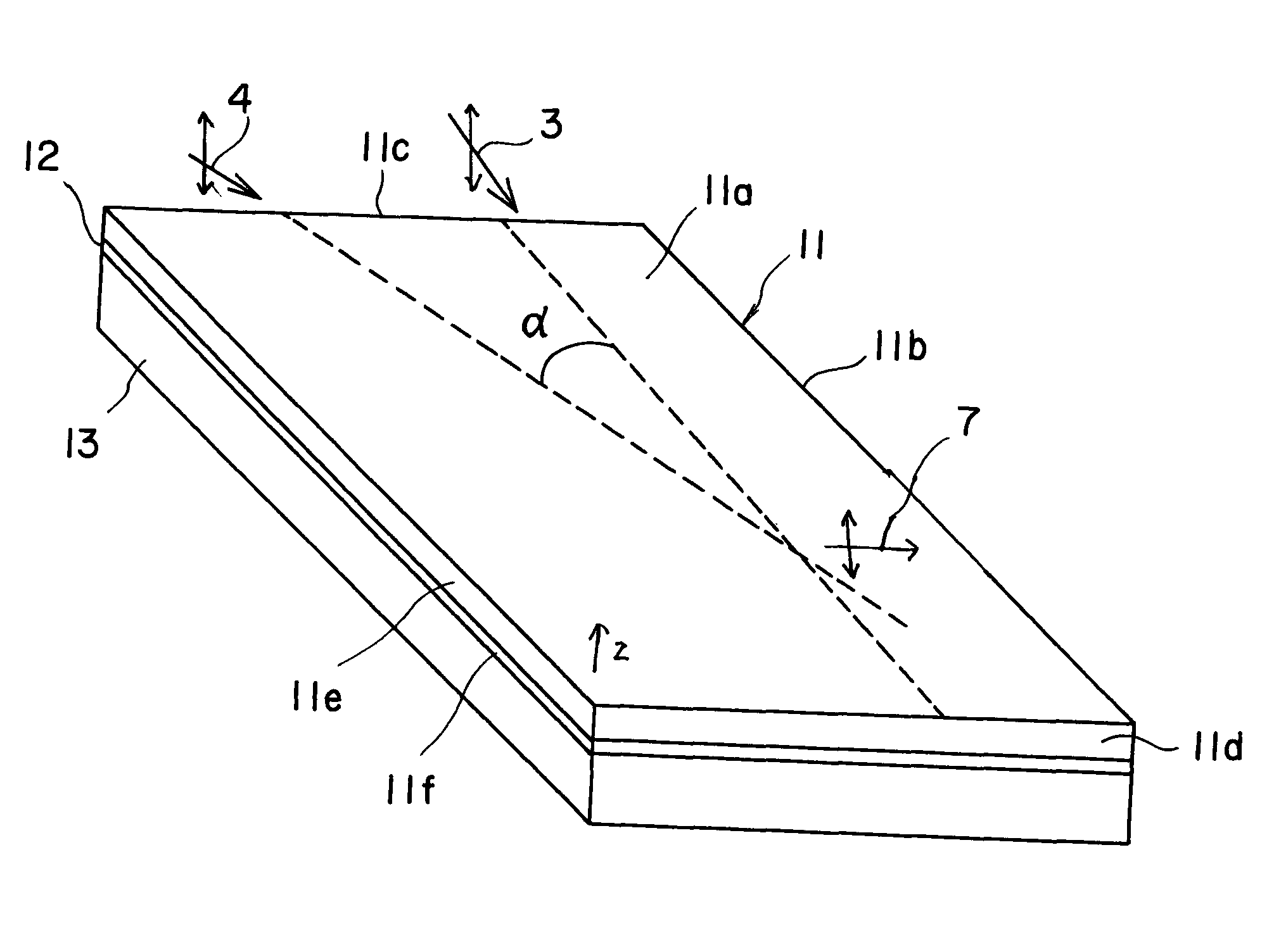
[0069]Specifically, a z-plate of lithium niobate single crystal doped with MgO was used as the oscillating substrate 11 and a z-plate of non-doped lithium niobate single crystal was used as the supporting body 13. The oscillating substrate has a refractive index of 2.14 with respect to the pump wave (wavelength of 1064 nm). An adhesive layer was applied onto the joining face of the supporting body in a thickness of 1 μm or smaller to adhere the z-plate of MgO-doped lithium niobate thereon. The adhesive layer used was made of a Cardo polymer and had a refractive index of 1.9 in a wavelength band of 1 μm. Then, the z-plate of MgO-doped lithium niobate was thinned by precise polishing to a thickness of 5 μm to form the oscillating substrate 11. Thereafter, the joined body was cut with a dicer to chips each having a length of 5 mm to produce the device shown in FIGS. 3,...

##ventive example 2

Inventive Example 2

[0073]The device described referring to FIGS. 3, 4 and 5(b) was produced, according to the same procedure described the Inventive Example 1. According to the present example, however, the film reflecting the electromagnetic wave was formed on the surface of the supporting body 13, before the supporting body 13 was adhered to the oscillating substrate 11. The adhesive layer was same as that described in the Inventive Example 1.

[0074]That is, on the joining surface of the supporting body of the z-plate of non-doped lithium niobate single crystal, titanium, platinum and gold were formed by vapor deposition in thicknesses of 100 angstrom, 200 angstrom and 1 μm, respectively. Then, platinum and titanium were formed in thicknesses of 200 and 100 angstrom, respectively, for further improving the adhesive strength to form the reflective film 15. The reflectivity of the thus formed refractive film was measured by a Fourier Transform Infrared Spectroscopy system (for exampl...


PUM

PropertyMeasurementUnit
thicknessaaaaaaaaaa
refractive indexaaaaaaaaaa

Abstract

A device for oscillating an electromagnetic wave having a frequency of 0.1 THz to 3 THz from pump and idler waves by a parametric effect. The device includes a supporting body, an oscillating substrate made of a non-linear optical crystal, and an adhesive layer adhering the supporting body and oscillating substrate. The oscillating substrate includes an upper face, a bottom face and an incident face on which the pump wave is made incident. The oscillating substrate provides cut-off with respect to the electromagnetic wave oscillated by the parametric effect when the pump and idler waves propagate in parallel with the bottom face.

Description

[0001]This application claims the benefit of Japanese Patent Application P2009-185768 filed on Aug. 10, 2009, the entirety of which is incorporated by reference.FIELD OF THE INVENTION[0002]The present invention relates to a device of oscillating so-called terahertz wave.BACKGROUND OF THE INVENTION[0003]Terahertz waves are electromagnetic waves generally having a frequency of 0.1 THz to 10 THz, and are expected for basic fields such as physical properties, electrospectroscopy, bioscience, chemistry and pharmaceutical science and for applied fields of atmospheric environmental assessment, security, material test, food test and communication.[0004]As a device for oscillating terahertz waves, it has been developed a backward wave oscillator (BOW) and photomixing in several hundreds GHz band and free electron energy laser, p-Ge laser and quantum cascade laser (QCL) for 1 THz or more. These devices, however, have problems in the miniaturization and improvement of output power.[0005]On the...

Claims


Application Information

Patent Timeline
Patent Type & Authority Patents(United States)
IPC IPC(8): G02F1/35
CPCG02F1/39G02F2203/13
Inventor KONDO, JUNGOAOKI, KENJIIWATA, YUICHIEJIRI, TETSUYA
Owner NGK INSULATORS LTD
Why Eureka
Try Eureka