
Method of programming nonvolatile semiconductor memory device

a nonvolatile, memory device technology, applied in static storage, digital storage, instruments, etc., can solve problems such as loss of stored data, and achieve the effect of reducing programming interferen

Active Publication Date: 2012-11-27
SAMSUNG ELECTRONICS CO LTD
View PDF9 Cites 13 Cited by
  • Summary
  • Abstract
  • Description
  • Claims
  • Application Information

AI Technical Summary

Benefits of technology

This method reduces programming interference between cell strings, ensuring accurate programming of selected memory cells while maintaining unprogrammed states in unselected cells, thereby enhancing the programming efficiency of NAND-type flash memory devices.

Problems solved by technology

The volatile semiconductor memory device may only store or read data while power is supplied and will lose the stored data when the power is interrupted.

Method used


Image

  • Method of programming nonvolatile semiconductor memory device
  • Method of programming nonvolatile semiconductor memory device
  • Method of programming nonvolatile semiconductor memory device

Examples


Embodiment Construction

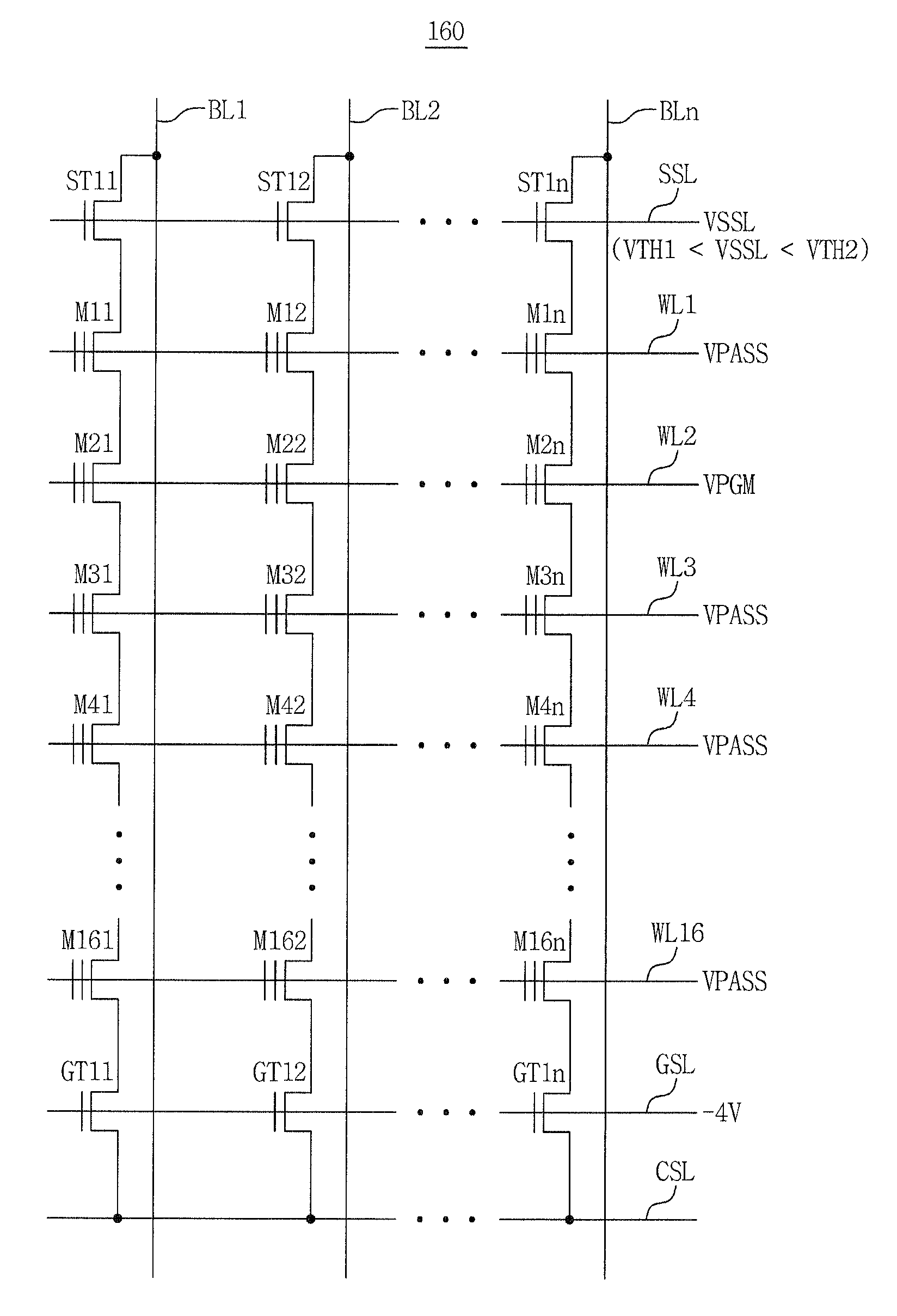
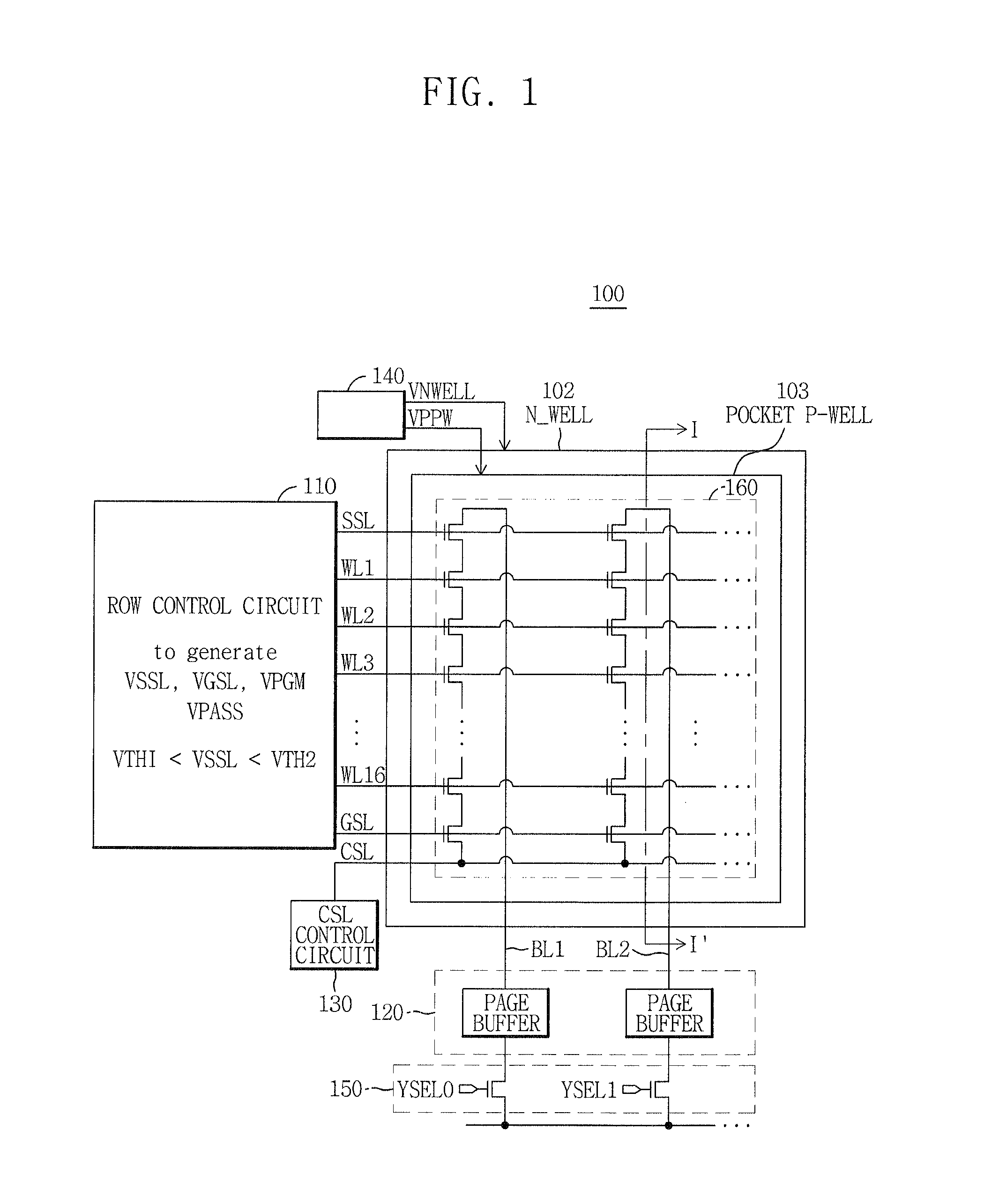
[0043]FIG. 1 is a block diagram of a NAND-type flash memory device according to an exemplary embodiment of the inventive concept.

[0044]Referring to FIG. 1, a NAND-type flash memory device 100 includes a row control circuit 110, a page buffer circuit 120, a common source line control circuit 130, a well bias circuit 140, a column gate circuit 150, and a memory cell array 160.

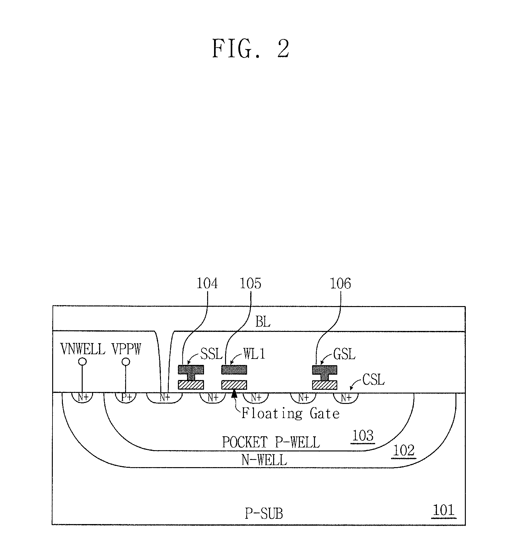
[0045]The memory cell array 160 may be formed in a pocket p-well region (POCKET P-WELL 103), which may be formed in a deeper well (N-WELL 102) formed in a bulk substrate. When the deep well has n-type conductivity, the pocket p-well may be formed to have p-type conductivity. Alternatively, the memory cell array 160 may be directly formed in the bulk substrate without the pocket / well structure.

[0046]The row control circuit 110 may generate a program voltage VPGM, a pass voltage VPASS, and a first voltage VSSL. The first voltage VSSL (a string selection line voltage) may have a voltage level higher than the thresho...


PUM


Abstract

A method of programming a nonvolatile semiconductor memory device using a negative bias voltage. The method includes turning ON the string selection transistors connected to selected bit lines and turning OFF the string selection transistors connected to unselected bit lines in the same memory block, in a program mode. This can be achieved by applying a negative bias voltage to a bulk substrate and applying a voltage having a voltage level higher than the threshold voltage of string selection transistors connected to selected bit lines and lower than the threshold voltage of string selection transistors connected to unselected bit lines. The method may reduce programming disturbance between a selected cell string and an unselected cell string.

Description

CROSS-REFERENCE TO RELATED APPLICATION[0001]This application claims priority, under 35 U.S.C. §119, of Korean Patent Application No. 10-2010-0006019 filed on Jan. 22, 2010, which is hereby incorporated by reference in its entirety.BACKGROUND[0002]1. Field[0003]The inventive concept relates to a method of programming a nonvolatile memory device and, more particularly, to a method of programming a NAND-type semiconductor flash memory device using a negative bias voltage.[0004]2. Description of Related Art[0005]Semiconductor memory devices may be largely classified into volatile memory devices and nonvolatile memory devices. A volatile memory device may store data as the logic state of a bistable flip-flop or as the charge stored in a capacitor. The volatile semiconductor memory device may only store or read data while power is supplied and will lose the stored data when the power is interrupted. The nonvolatile semiconductor memory device may be used to store programs and data in a wi...

Claims


Application Information

Patent Timeline
Patent Type & Authority Patents(United States)
IPC IPC(8): G11C16/04
CPCG11C16/10G11C16/0483G11C16/12
Inventor YANG, SEUNG-JINKIM, YONG-TAE
Owner SAMSUNG ELECTRONICS CO LTD
Learn More