Dual data rate flip-flop circuit

a flip-flop circuit and data rate technology, applied in the field of electric circuits, can solve problems such as undesirable changes in logic state of such circuits and changes in circuit logic states

Active Publication Date: 2012-12-04
STC UNM
View PDF1 Cites 16 Cited by
  • Summary
  • Abstract
  • Description
  • Claims
  • Application Information

AI Technical Summary

Benefits of technology

[0022]The DDR flip-flop circuit also includes an output buffer inverter connected to the extended C-element output. The output buffer inverter has an output that is the flip-flop circuit output. At least one internal keeper circuit is connected to the plurality of C-elements. A C-element keeper circuit is also connected to the C-element output. Advantageously, the present circuit also provides immunity from SEU events.

Problems solved by technology

SEUs can alter a node voltage in a circuit, which can result in changes in logic states of the circuit.
Many of these circuits are used for memory storage, and any changes in the logic states of such circuits are undesirable since they alter values stored in the memory.

Method used


Image

  • Dual data rate flip-flop circuit
  • Dual data rate flip-flop circuit
  • Dual data rate flip-flop circuit

Examples


Embodiment Construction

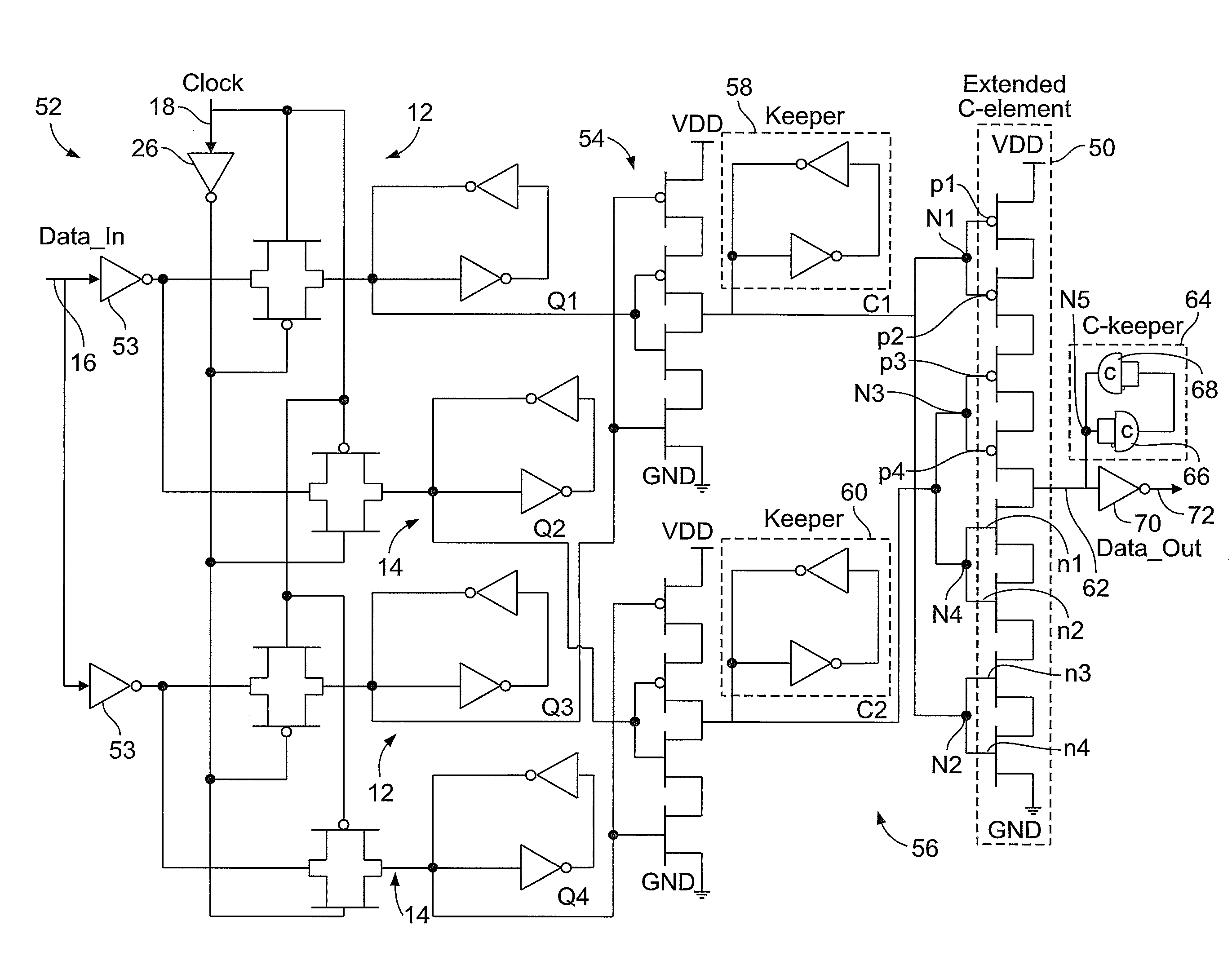
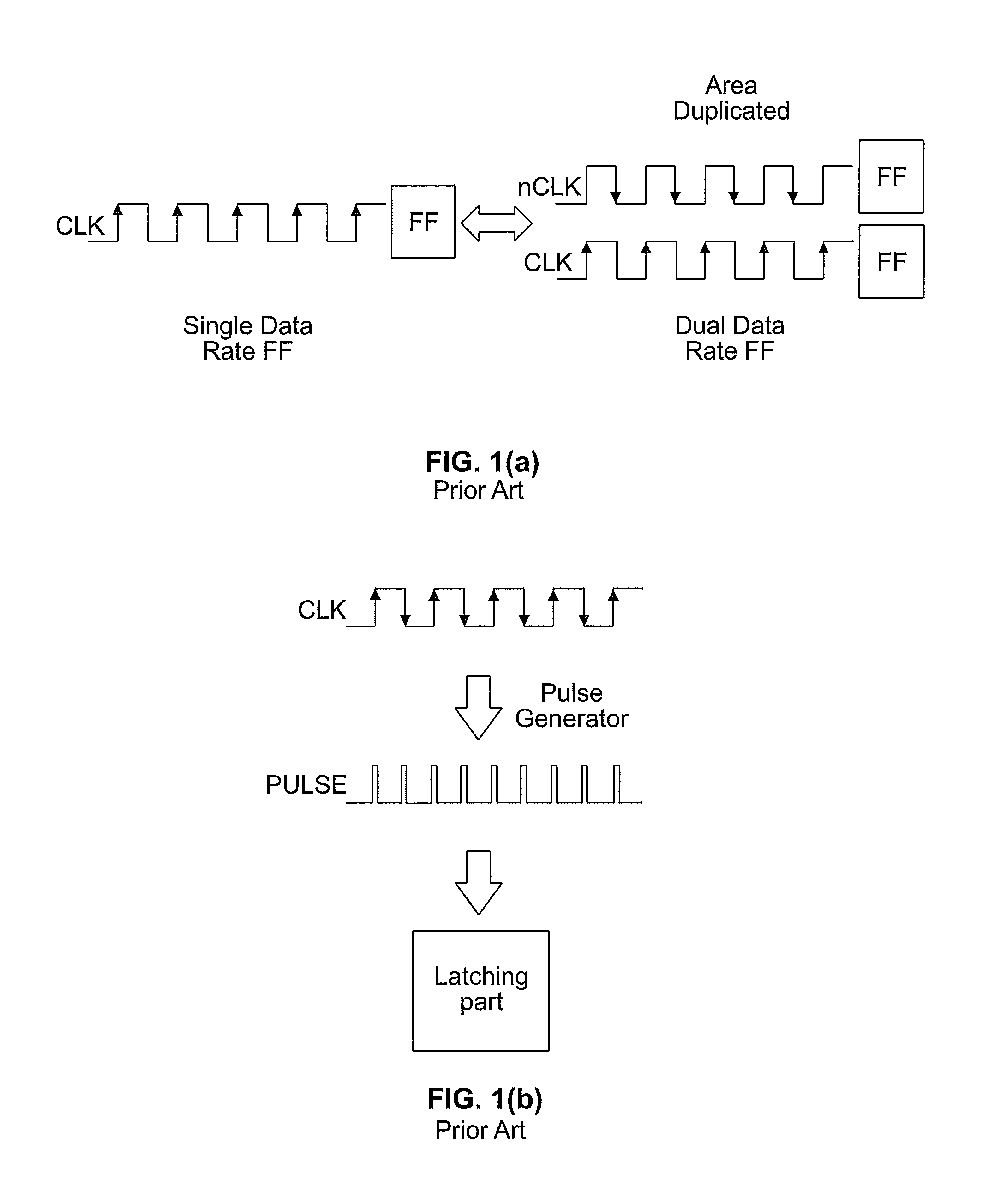
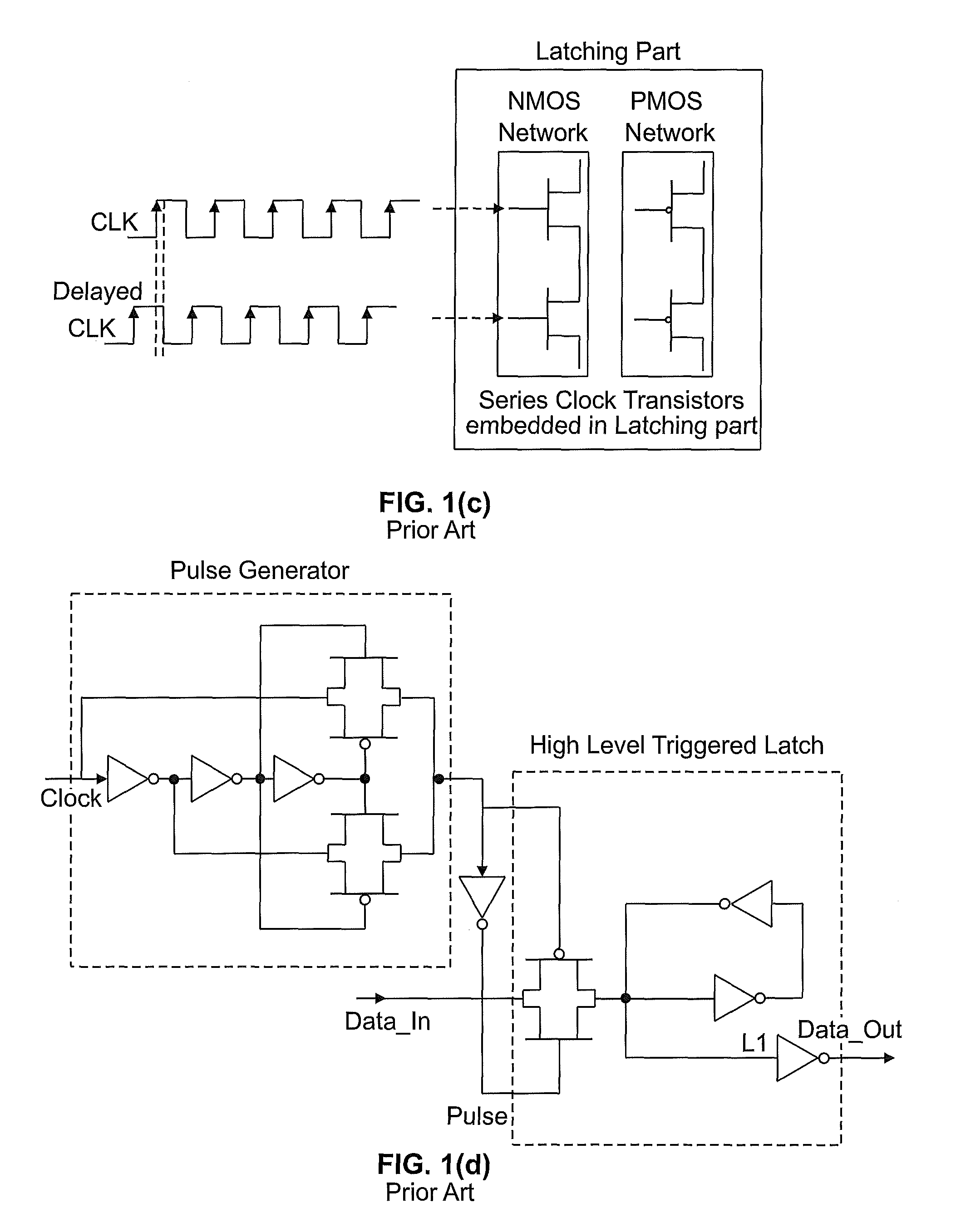
[0040]Flip-flop circuits are widely used in digital circuits to store data. The power, delay, and reliability of the flip-flop circuits directly affect the performance and fault tolerance of the whole integrated circuit formed on a semiconductor chip. Therefore, it is imperative to carefully design flip flop circuits for minimum area, delay, power, and maximum reliability. DDR flip-flop circuits are preferred to enhance the data throughput and to reduce the power consumption of application specific integrated circuit (ASIC) chips. Unlike a regular flip-flop circuit, which stores the input data on only the rising edge of a clock pulse, a DDR flip-flop circuit stores the input data on both rising and falling edges of the clock pulse, which leads to a higher data throughput for the same clock frequency.

[0041]A new and robust DDR flip-flop circuit with low power consumption is provided. The DDR flip-flop circuit has a very low activity factor due to its hard edge property and low clock ...


PUM


Abstract

A dual data rate flip-flop circuit for reducing single event upset errors in the flip-flop circuit including two or more latch circuits connected in parallel. The latch circuits each have a clock input, data input, and latch circuit output. The dual data rate flip-flop circuit also includes a C-element, which has a plurality of inputs and a C-element output. The outputs of the latch circuits are provided to inputs of the C-element, and a keeper circuit is connected to the C-element output. An output buffer inverter connects to the C-element output and has an output corresponding to the dual data rate flip-flop circuit output.

Description

[0001]This application claims the benefit of U.S. Provisional Patent Application Ser. No. 61 / 342,031 filed Apr. 8, 2010, the disclosure of which is incorporated herein by reference in its entirety.GOVERNMENT FUNDING[0002]The invention described herein was made with government support under grant number FA 9453-08-2-0259, awarded by the Air Force Research Laboratory. The United States Government may have certain rights in the invention.FIELD OF THE INVENTION[0003]The present invention generally relates to electrical circuits including in integrated circuits, and in particular to dual data rate flip-flop circuits.BACKGROUND OF THE INVENTION[0004]Electrical or digital logic circuits that include flip-flop architectures are increasingly being reduced in size to accommodate the increasing number of electrical circuits formed on semiconductor chips. This is known as circuit scaling, which has reduced gate capacitance thereby increasing sensitivity to radiation induced soft errors. Circuit...

Claims


Application Information

Patent Timeline
Patent Type & Authority Patents(United States)
IPC IPC(8): H03K3/00
CPCH03K3/0375
Inventor ZARKESH-HA, PAYMANDEVARAPALLI, VALLABH SRIKANTHSUDDARTH, STEVEN C.
Owner STC UNM
Why Eureka
Try Eureka