Bipolar transistor having base over buried insulating and polycrystalline regions

a bipolar transistor and polycrystalline technology, applied in the field of electric systems and semiconductor devices, can solve the problems of lower collector resistance, achieve the effects of avoiding alignment tolerance inherent, better control of base resistance, and better control of gain and bandwidth

Active Publication Date: 2007-02-20
TEXAS INSTR INC
View PDF7 Cites 2 Cited by
  • Summary
  • Abstract
  • Description
  • Claims
  • Application Information

AI Technical Summary

Benefits of technology

[0004]A need has therefore arisen to conceive a fresh concept of a coherent, low-cost methodology for fabricating bipolar, and specifically heterojunction bipolar, transistors using fewer photomasks and maintaining alignment features such as self-aligned emitter-to-base polysilicon and aligned collector. Avoiding the alignment tolerance inherent in the use of photomasks, the base resistance can be better controlled, which translates into a better control of gain and bandwidth. In addition, having the base over oxide lowers the base-to-collector capacitance and provides immunity to cosmic radiation faults.
[0005]It is a technical advantage of the new fabrication concept that it is based on fundamental design concepts, which are flexible enough to be applied for different semiconductor product families and a wide spectrum of design variations. It is another technical advantage that, due to a reduction of photomasks the process yield is enhanced, while the innovations are accomplished using the installed equipment base so that no investment in new manufacturing machines is needed.
[0006]One embodiment of the invention is a bipolar transistor in a monocrystalline semiconductor substrate, which has a first conductivity type and includes a surface layer of the opposite conductivity type. The transistor comprises an emitter contact on the surface layer; a base contact extending through a substantial portion of the surface layer, spaced apart from the emitter; an insulator region buried under the base contact; a collector contact; and a first polycrystalline semiconductor region selectively located under the insulator region, and a second polycrystalline semiconductor region selectively located under the collector contact. These polycrystalline regions exhibit heavy dopant concentrations of the first conductivity type; consequently, they lower the collector resistance.
[0008]Another embodiment of the invention is a method for fabricating a bipolar transistor, or a heterojunction bipolar transistor (HBT) comprising chemical-mechanical polishing (CMP) techniques, which can be coordinated with CMOS CMP manufacturing. The process sequence entails several CMP steps to reduce the photomask count; compared to a standard HBT process sequence of eight mask steps, the invention requires only seven mask steps. In the fabrication method, trenches are employed to accommodate the base and collector contacts. The trenches are defined by silicon carbide walls, which also serve as stoppers in the chemical-mechanical polishing process steps. Due to the straight-line geometry of the trenches, components of base and collector assembled in those trenches in consecutive order, are by necessity completely aligned. Consequently, transistor characteristics such as parasitic and transverse base resistance, and collector resistance, can be strictly controlled, resulting in devices suitable for applications requiring higher gain and bandwidth.

Problems solved by technology

These polycrystalline regions exhibit heavy dopant concentrations of the first conductivity type; consequently, they lower the collector resistance.

Method used


Image

  • Bipolar transistor having base over buried insulating and polycrystalline regions
  • Bipolar transistor having base over buried insulating and polycrystalline regions
  • Bipolar transistor having base over buried insulating and polycrystalline regions

Examples


Embodiment Construction

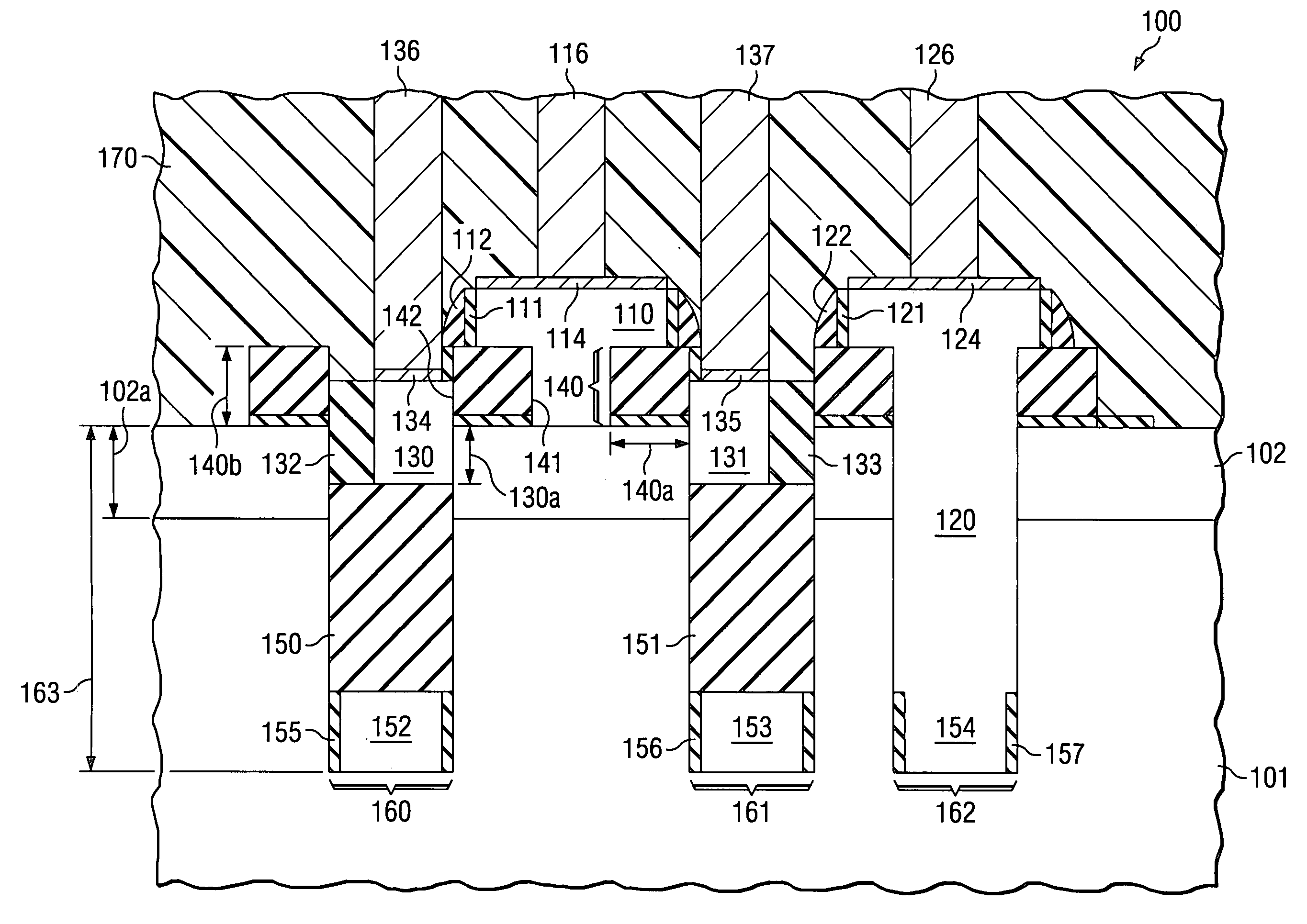
[0028]FIG. 1 illustrates a schematic cross section of a portion of a semiconductor substrate 101 depicting a heterojunction bipolar transistor (HBT) device, generally designated 100, according to an embodiment of the present invention. The semiconductor substrate is monocrystalline and has a first conductivity type. Preferably, the substrate is made of silicon and the conductivity is n-type; the considerations of this invention, however, also apply to p-type semiconductor substrate material, and to any other semiconductor material, including gallium arsenide, used in device production.

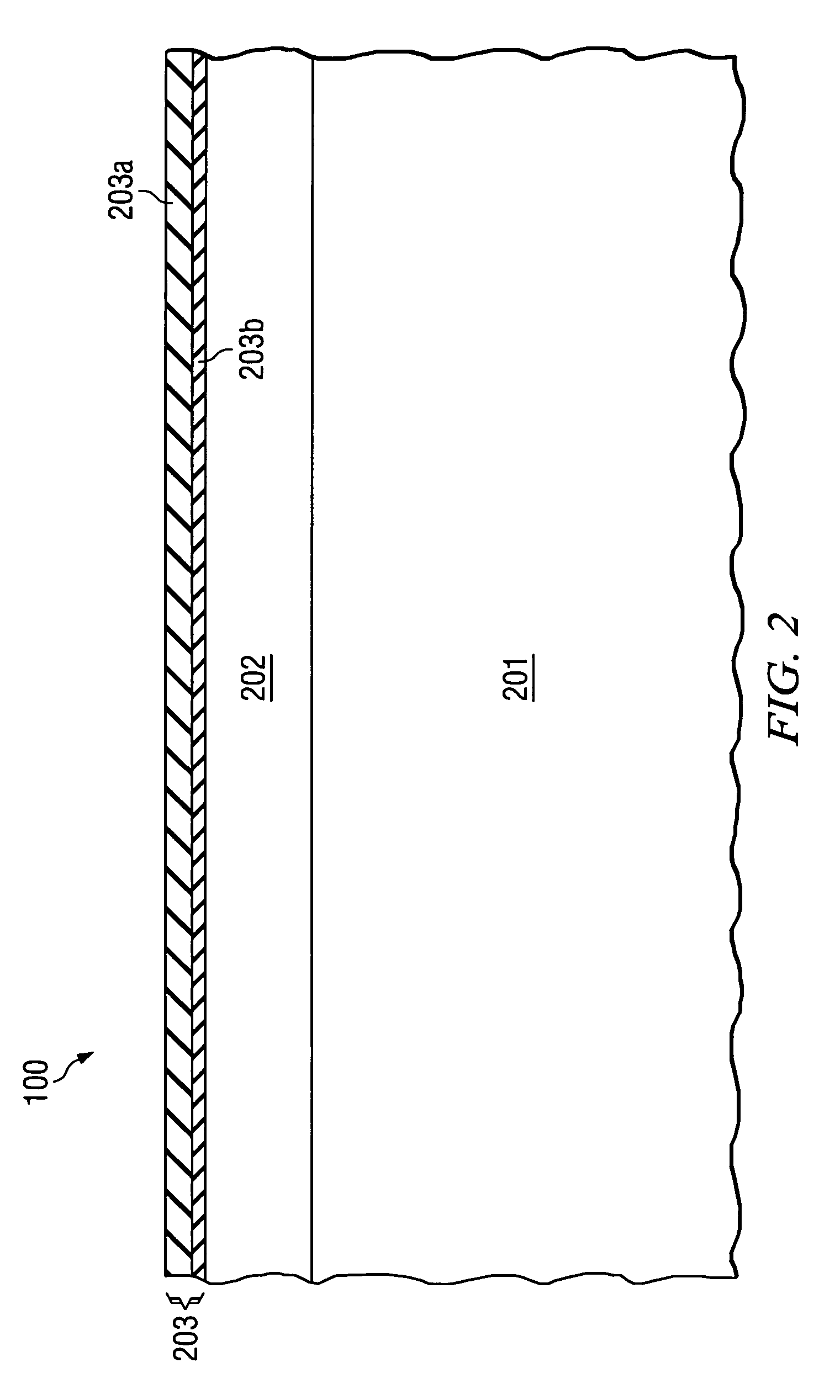
[0029]In the example of FIG. 1, the surface of substrate 101 is topped by a monocrystalline surface layer 102. This surface layer 102 is epitaxially grown and may have intrinsic conductivity or opposite conductivity type; it may be composed of the same semiconductor material as substrate 101 or it may be a different semiconductor. As examples, surface layer 102 may be p-type silicon on an n-type substr...


PUM


Abstract

A bipolar transistor in a monocrystalline semiconductor substrate (101), which has a first conductivity type and includes a surface layer (102) of the opposite conductivity type. The transistor comprises an emitter contact (110) on the surface layer; a base contact (130 and 131) extending through a substantial portion (141) of the surface layer, spaced apart (140a) from the emitter; an insulator region (150 / 151) buried under the base contact; a collector contact (120); and a first polycrystalline semiconductor region (152 / 153) selectively located under the insulator region, and a second polycrystalline semiconductor region (154) selectively located under the collector contact. These polycrystalline regions exhibit heavy dopant concentrations of the first conductivity type; consequently, they lower the collector resistance.

Description

FIELD OF THE INVENTION[0001]The present invention is related in general to the field of electrical systems and semiconductor devices and more specifically to structure and method of a low-cost, low base / collector capacitance, high gain bipolar transistor having its base over buried insulator and polycrystalline regions.DESCRIPTION OF THE RELATED ART[0002]The bipolar transistor is one of the most important semiconductor devices and a fundamental building block of integrated circuits (IC), with applications in computers, vehicles, satellites, and in communication and power systems. Because of its widespread use, it is subject to the dominating on-going market trends: progressive integration of functions, downscaling of dimensions, increase of speed, power, and reliability, and last, but not least, downsizing cost.[0003]It is common practice to propose improvements on one subject or the other, one at a time: either a technical parameter, or a commercial projection, or a manufacturing n...

Claims


Application Information

Patent Timeline
Patent Type & Authority Patents(United States)
IPC IPC(8): H01L29/737
CPCH01L29/0649H01L29/0821G08C17/02H01L29/41708H01L29/732H01L29/1004H01L21/8249
Inventor HOWARD, GREGORY E.
Owner TEXAS INSTR INC
Why Eureka
Try Eureka