

Semiconductor process having dielectric layer including metal oxide and MOS transistor process
a technology of dielectric layer and semiconductor, applied in the direction of semiconductor devices, basic electric elements, electrical equipment, etc., can solve the problems of reducing gate capacitance, inferior performance, and conventional polysilicon gates, and achieve the effect of reducing threshold voltage and improving electrical quality
- Summary
- Abstract
- Description
- Claims
- Application Information
AI Technical Summary
Benefits of technology
Problems solved by technology
Method used
Image

Examples
first embodiment
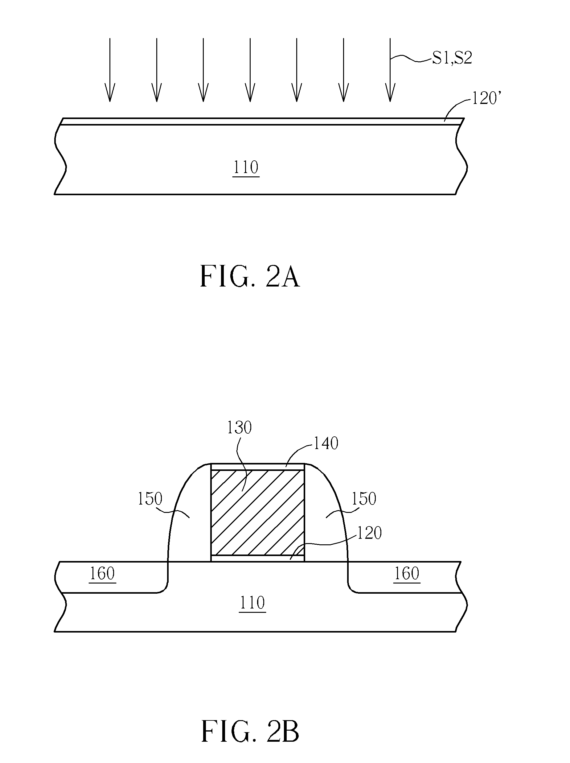
[0030]As shown in FIG. 2B, a metal layer (not shown) such as aluminum (Al) or other metals is formed on the dielectric layer 120′. A cap layer (not shown) is selectively formed on the metal layer. A photo-etching process is applied to pattern the cap layer and then the patterned cap layer 140, the metal gate 130 and the gate dielectric layer 120 can be sequentially formed. The spacer 150 with single or multi composite structure is formed beside the gate dielectric layer 120 and the metal gate 130. An ion implantation process and junction activation annealing process etc. are performed to form a source / drain region 160 next to the spacer 150 (as shown in FIG. 2B). In this embodiment, a silicon epitaxial process may be selectively performed and a metal silicide process, a contact etch stop layer (CESL) process etc. may be preformed on the source / drain region 160, meaning the MOS transistor process in this invention is finished, wherein the gate first process is applied in the MOS tran...
second embodiment
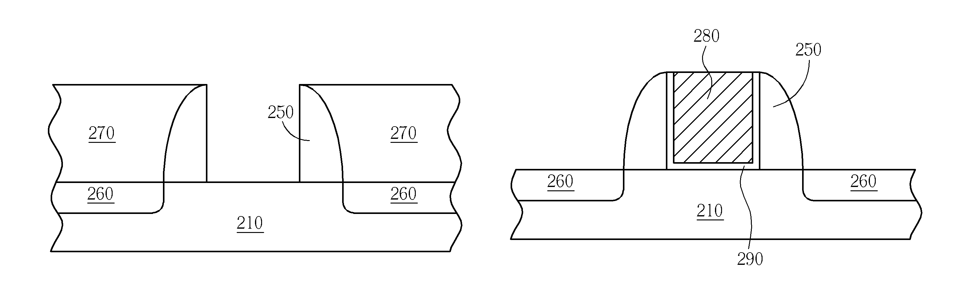
[0031]FIG. 3A-3E schematically depict a cross-sectional view of a MOS transistor process according to a second preferred embodiment of the present invention. Referring to FIG. 3A-3E, a substrate 210 is provided. A dielectric layer 220′ having a high-k dielectric constant is formed on the substrate 210, wherein the dielectric layer 220′ may be metal oxide (as shown in 3A) and a buffer layer may be selectively contained. A silicon layer (not shown), a polycrystalline silicon layer for instance, is formed in the dielectric layer 220′. A cap layer (not shown) is selectively formed on the silicon layer. A photo etching process is performed to pattern the cap layer for sequentially form a patterned cap layer 240, a silicon gate electrode 230 and a gate dielectric layer 220. In this embodiment, the silicon gate electrode 230 and the cap layer 240 are used as a sacrificed gate structure. A spacer 250 with single or multi composite structure is formed beside the gate dielectric layer 220, th...
PUM
| Property | Measurement | Unit |
|---|---|---|
| temperature | aaaaa | aaaaa |
| temperature | aaaaa | aaaaa |
| temperature | aaaaa | aaaaa |
Abstract
Description
Claims
Application Information