Apparatus and method for improving photoresist properties using a quasi-neutral beam

a quasi-neutral beam and apparatus technology, applied in the field of substrate processing, can solve the problems of electrically charged particles, semiconductor structure tolerance, semiconductor device manufacturing, etc., and achieve the effect of eliminating line edge roughness (ler) and line width roughness

a quasi-neutral beam and apparatus technology, applied in the field of substrate processing, can solve the problems of electrically charged particles, semiconductor structure tolerance, semiconductor device manufacturing, etc., and achieve the effect of eliminating line edge roughness (ler) and line width roughness

US8343371B2Inactive Publication Date: 2013-01-01TOKYO ELECTRON LTD

Image

  • Apparatus and method for improving photoresist properties using a quasi-neutral beam
  • Apparatus and method for improving photoresist properties using a quasi-neutral beam
  • Apparatus and method for improving photoresist properties using a quasi-neutral beam

Examples


Embodiment Construction

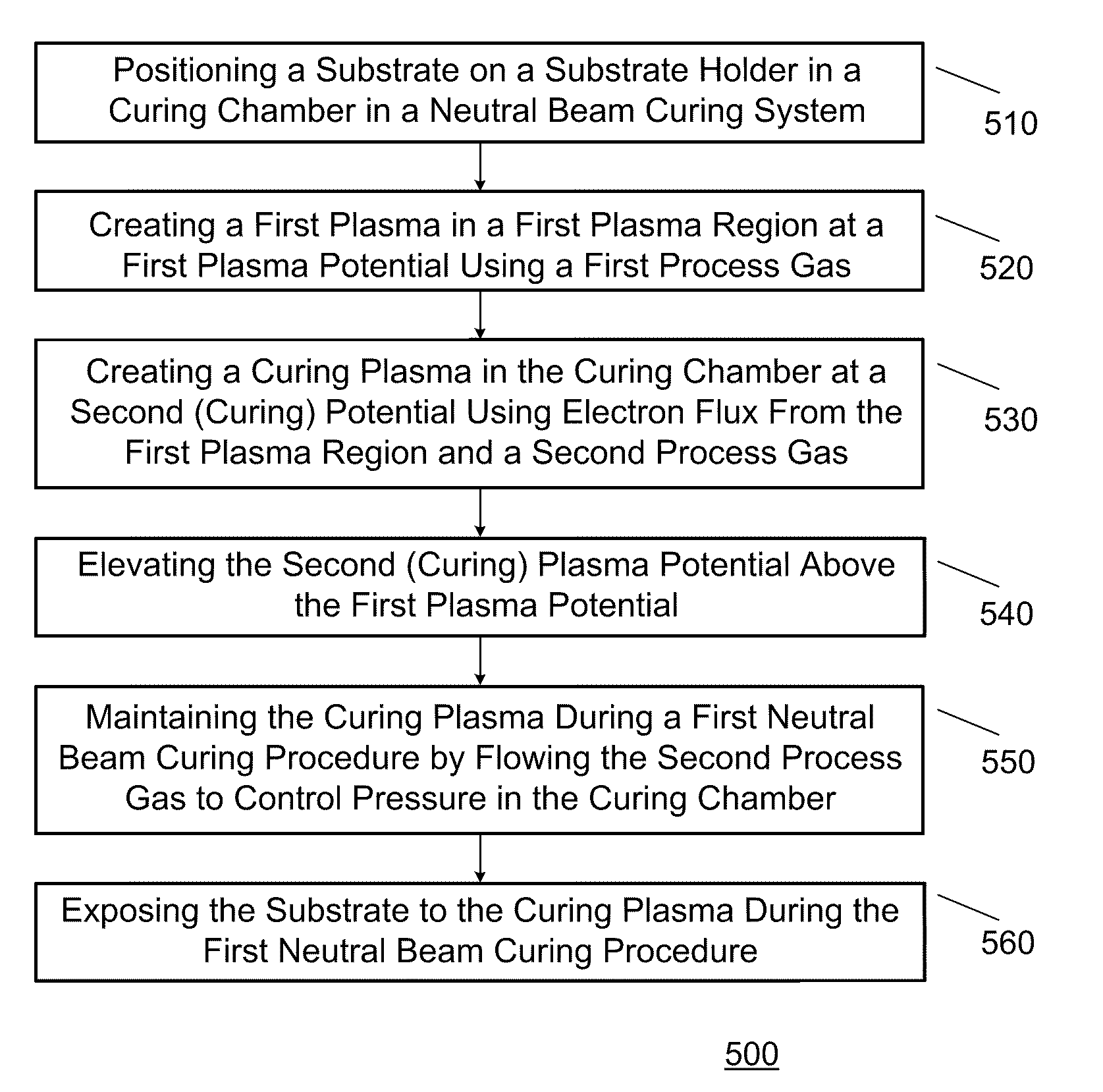
[0025]The invention provides apparatus and methods of processing a substrate in real-time using subsystems and processing sequences created to cure and / or harden radiation-sensitive materials. In addition, the cured and / or hardened radiation-sensitive material layer can be used to more accurately control gate and / or spacer critical dimensions (CDs), to control gate and / or spacer CD uniformity, and to eliminate and / or reduce line edge roughness (LER) and line width roughness (LWR).

[0026]In some embodiments, apparatus and methods are provided for creating and / or using a metrology library that includes profile data and diffraction signal data for cured and / or hardened radiation-sensitive material (photoresist) features and periodic structures.

[0027]One or more evaluation features can be provided at various locations on a substrate and can be used to evaluate and / or verify Q-NB curing (hardening) procedures and associated models. Substrates can have real-time and historical data associa...


PUM


Abstract

The invention can provide apparatus and methods of processing a substrate in real-time using a Quasi-Neutral Beam (Q-NB) curing system to improve the etch resistance of photoresist layer. In addition, the improved photoresist layer can be used to more accurately control gate and / or spacer critical dimensions (CDs), to control gate and / or spacer CD uniformity, and to eliminate line edge roughness (LER) and line width roughness (LWR).

Description

BACKGROUND OF THE INVENTION[0001]1. Field of the Invention[0002]The present invention relates to substrate processing, and more particularly to improving the substrate processing using radiation-sensitive material (photoresist) curing and / or hardening procedures, and subsystems.[0003]2. Description of the Related Art[0004]During semiconductor processing, plasma is often utilized to assist etch processes by facilitating the anisotropic removal of material along fine lines or within vias (or contacts) patterned on a semiconductor substrate. Furthermore, plasma is utilized to enhance the deposition of thin films by providing improved mobility of adatoms on a semiconductor substrate.[0005]Once the plasma is formed, selected surfaces of the substrate are etched by the plasma. The process is adjusted to achieve appropriate conditions, including an appropriate concentration of desirable reactant and ion populations to etch various features (e.g., trenches, vias, contacts, etc.) in the sele...

Claims


Application Information

Patent Timeline
01 Jan 2013
Publication
US8343371B2
IPC
G01L21/30
CPC
H01J37/32009; H01J37/3233; H01J37/32357; H01J37/32422; H01J37/3244; H01J37/32449; H01J37/32458; H01J37/32532
Inventors
FUNK, MERRITT; CHEN, LEE