Method to arrange features on a substrate to replicate features having minimal dimensional variability

a technology of features and substrates, applied in the field of patterning substrates, can solve the problems of low yield rate, time-consuming post-process characterization step, and difficulty in repeatably producing reliable accurate metrology standards, so as to minimize the thickness variation in the layer, minimize the dimensional variability of features, and reduce the effect of thickness variation

Active Publication Date: 2013-01-08
MOLECULAR IMPRINTS
View PDF489 Cites 132 Cited by
  • Summary
  • Abstract
  • Description
  • Claims
  • Application Information

AI Technical Summary

Benefits of technology

[0007]The present invention is directed to a method of and a mold for arranging features on a substrate to replicate the features while minimizing dimensional variability in the features. The method includes arranging features on a layer to minimize thickness variations in the layer that are attributable to density variations of the plurality of features on the layer. The features are transferred into an underlying substrate. Recognizing thickness variations in the patterned layer makes difficult controlling feature dimensions f

Problems solved by technology

This is due, in part, to the difficulty in repeatably producing reliable accurate metrology standards.
A drawback with the conventional processes for manufacturing metrology stand

Method used


Image

  • Method to arrange features on a substrate to replicate features having minimal dimensional variability
  • Method to arrange features on a substrate to replicate features having minimal dimensional variability
  • Method to arrange features on a substrate to replicate features having minimal dimensional variability

Examples


Embodiment Construction

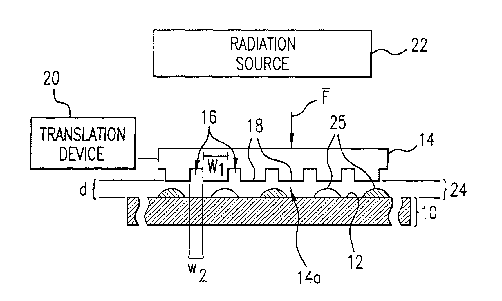
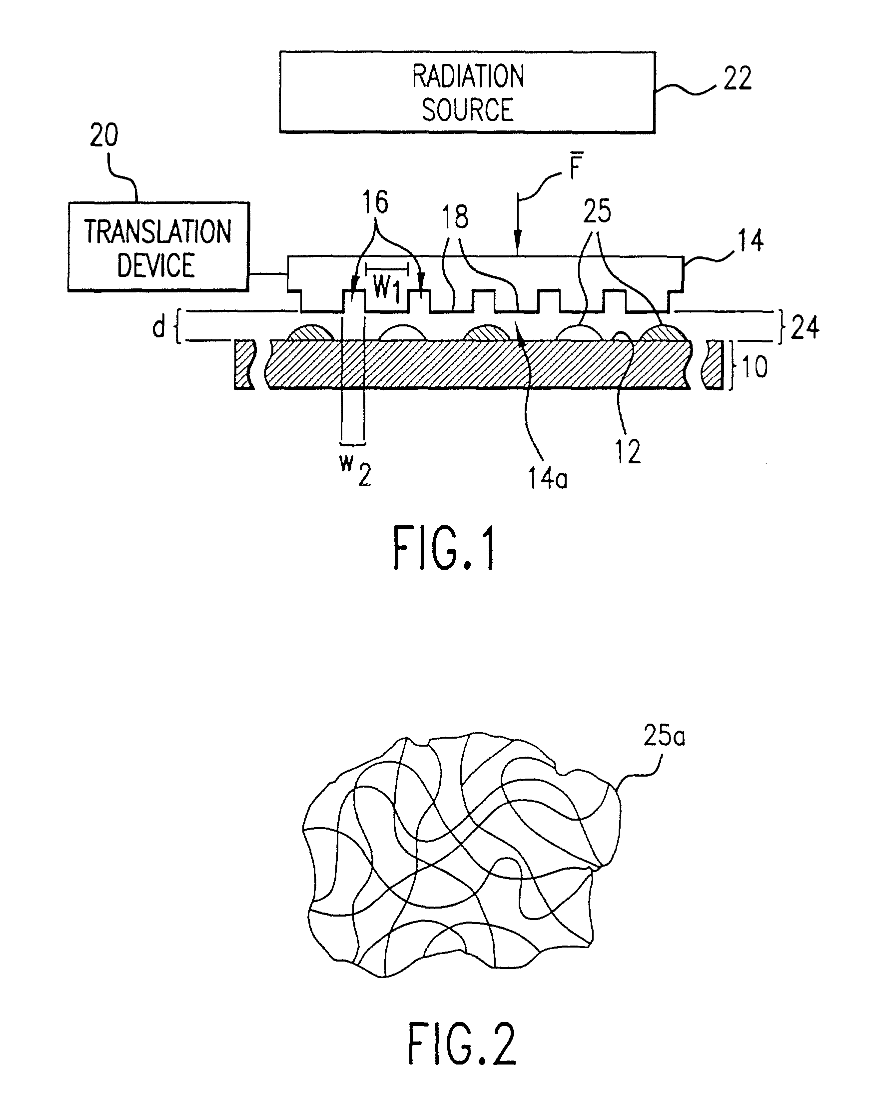
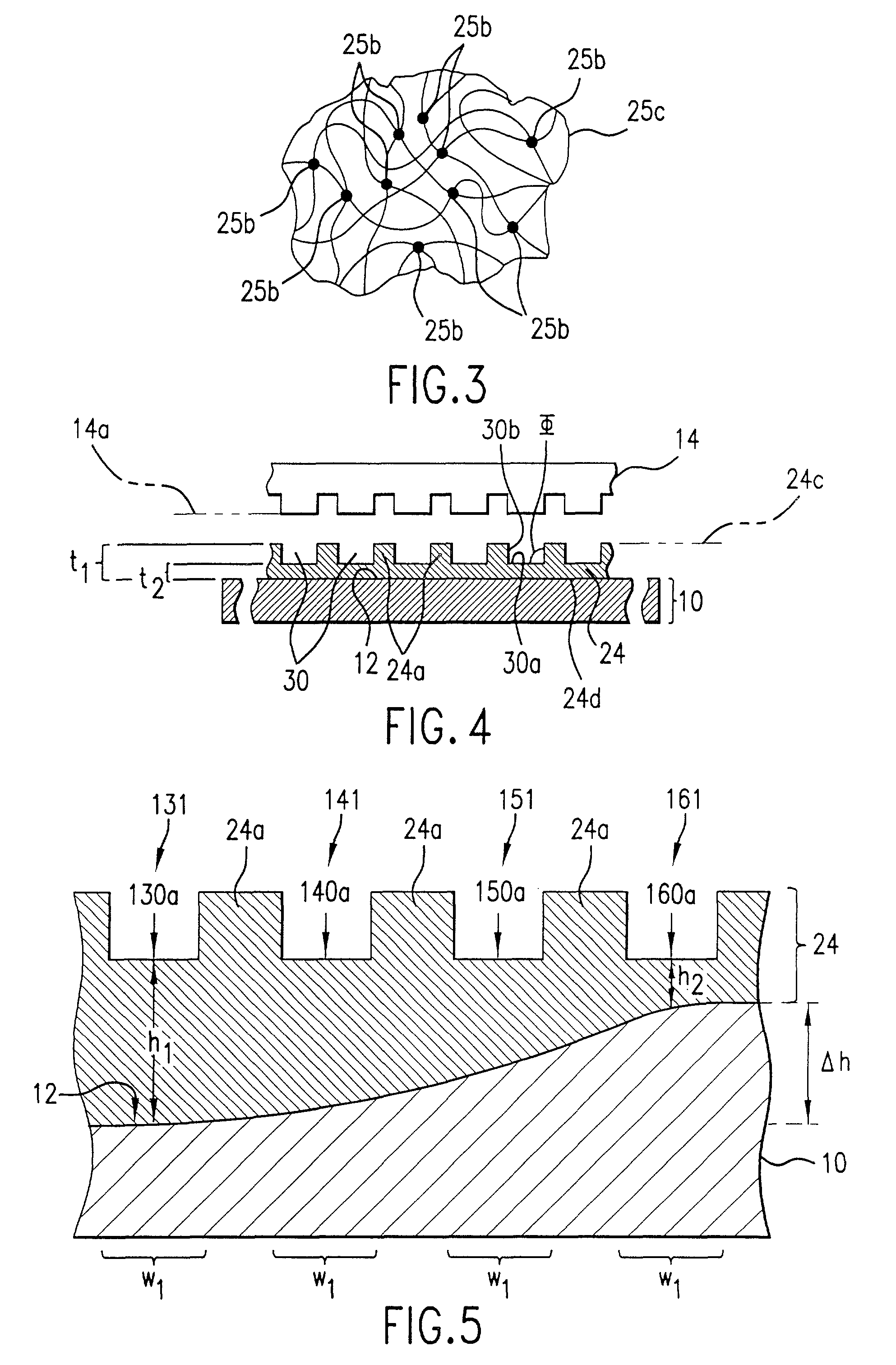
[0020]Referring to FIG. 1, a lithographic system in accordance with an embodiment of the present invention includes a substrate 10, having a substantially planar region shown as surface 12. Disposed opposite substrate 10 is an imprint device, such as a mold 14, having a plurality of features thereon, forming a plurality of spaced-apart recessions 16 and protrusions 18. In the present embodiment, recessions 16 are a plurality of grooves extending along a direction parallel to protrusions 18 that provide a cross-section of mold 14 with a shape of a battlement. However, recessions 16 may correspond to virtually any feature required to create an integrated circuit. A translation device 20 is connected between mold 14 and substrate 10 to vary a distance “d” between mold 14 and substrate 10. A radiation source 22 is located so that mold 14 is positioned between radiation source 22 and substrate 10. Radiation source 22 is configured to impinge radiation on substrate 10. To realize this, mo...


PUM

PropertyMeasurementUnit
Volumeaaaaaaaaaa
Volumeaaaaaaaaaa
Volumeaaaaaaaaaa

Abstract

The present invention is directed to a method of and a mold for arranging features on a substrate to replicate the features with minimal dimensional variability. The method includes arranging features on a layer to minimize thickness variations in the layer that are attributable to density variations of the plurality of features on the layer. The features are transferred into an underlying substrate. It is believed that by forming the features so as to define a uniform fill factor in the layer, the thickness variations may be reduced, if not abrogated. To that end, one method in accordance with the present invention includes forming a flowable material on the substrate. Thereafter, a plurality of features is formed in a region of the flowable material. The plurality of features are arranged to provide a substantially uniform fill factor in the region.

Description

[0001]The field of invention relates generally to patterning substrates. More particularly, the present invention is directed to arranging features on a substrate to minimize dimensional variability among the features.[0002]Control features dimensions formed during semiconductor processes is highly desired. In this manner, features may be fabricated having tightly controlled dimensional variations, i.e., variability from the desired dimensions is minimized. Features formed with tightly controlled dimensional variations are used for many purposes, including metrology standards.[0003]Metrology standards are employed in many industries to measure the operation of varying equipment and processes. For semiconductor processes, a typical metrology standard may include grating structures, L-shaped structures and other common patterning geometries found on production devices. In this manner, the metrology standards facilitate measurement of the performance of the processing equipment.[0004]C...

Claims


Application Information

Patent Timeline
IPC IPC(8): B29C35/00B29C43/00B29C35/08B29C59/02G03F1/00G03F7/00
CPCB29C43/003B29C59/022G03F7/0002B82Y10/00B82Y40/00B29C2035/0827B29C2035/0833B29C2059/023B29C2043/025
Inventor SREENIVASAN, SIDLGATA V.WATTS, MICHAEL P. C.
Owner MOLECULAR IMPRINTS
Why Eureka
Try Eureka