Composite substrate, EL panel using the same, and making method
a technology of composite substrate and el panel, applied in the field of el panel, can solve the problems of limited use of el panel, difficult to manufacture el panel displays having large surface area, structural problems still unsolved, etc., and achieve the effect of preventing any variation of el light emission, minimizing surface asperities, and minimizing thickness variation of pzt which has been fired for smoothing
- Summary
- Abstract
- Description
- Claims
- Application Information
AI Technical Summary
Benefits of technology
Problems solved by technology
Method used
Image
Examples
example
[0101]Examples of the invention are given below by way of illustration and not by way of limitation.
example a-1
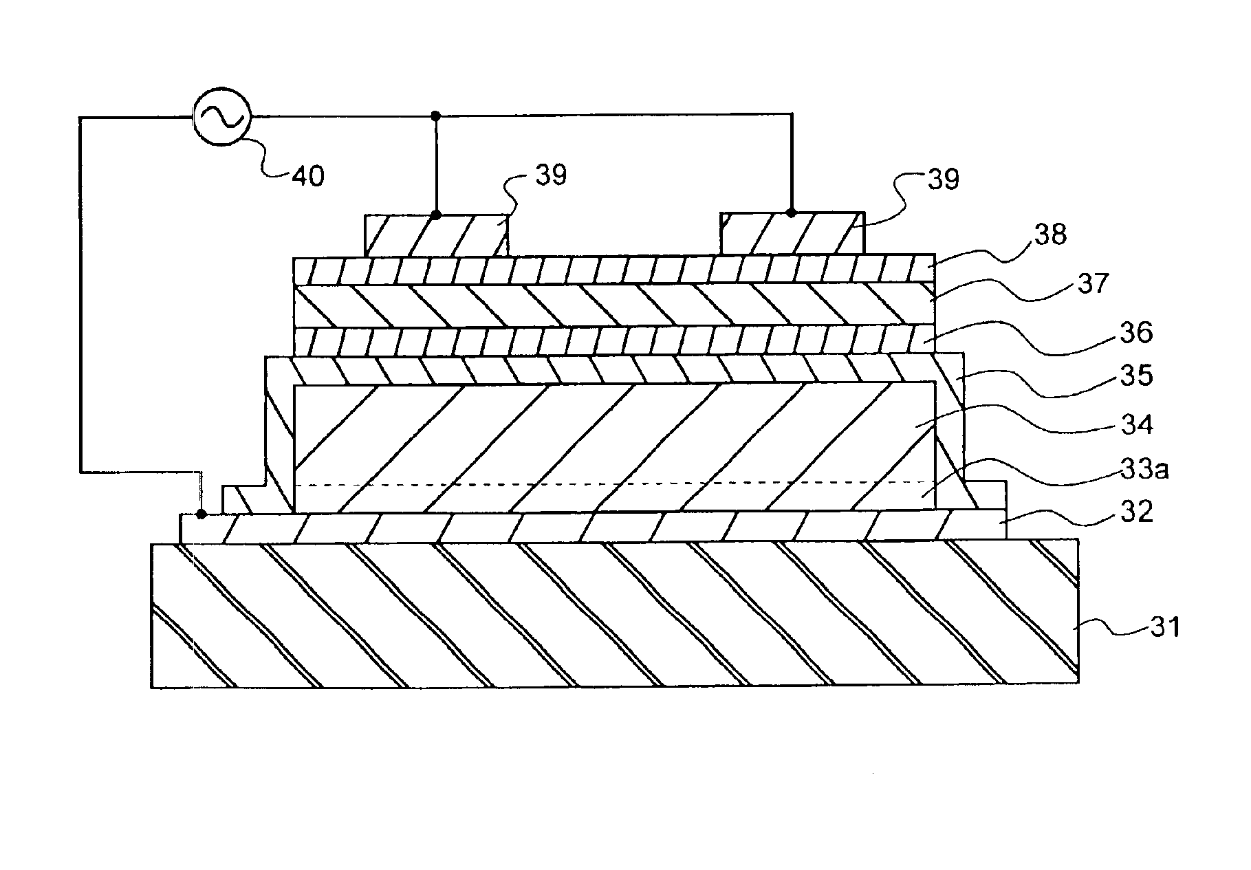
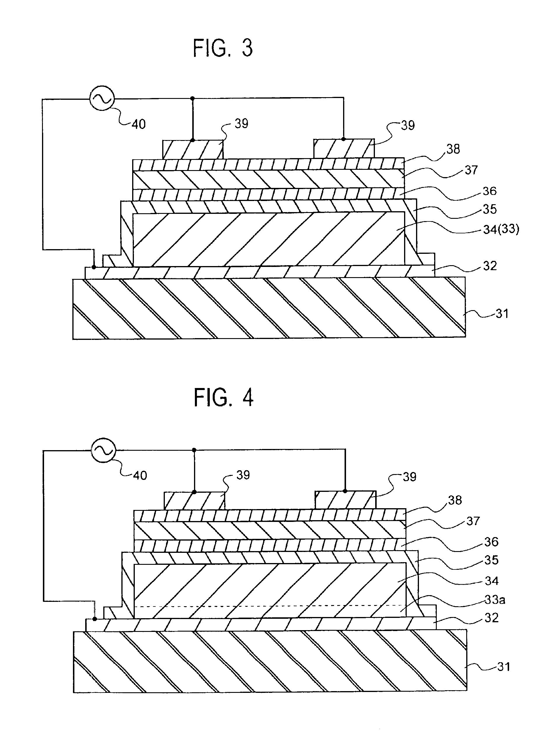
[0102]On a 96% pure alumina substrate, an Au thin film having trace additives added thereto was formed to a thickness of 1 μm by a sputtering technique. It was annealed at 850° C. for stabilization. The lower electrode layer of Au was patterned in a plurality of stripes having a width of 300 μm and a space of 30 μm by a photo-etching technique.
[0103]On the substrate having the lower electrode formed thereon, a dielectric ceramic thick film was formed by a screen printing technique. The thick film paste used was thick-film dielectric paste 4210C by ESL. Screen printing and drying steps were repeated such that a film thickness of 5 μm was obtained at the end of firing.
[0104]After the printing and drying steps, the thick film was fired in a belt furnace having a full air feed atmosphere at 850° C. for 20 minutes.
[0105]Next, a dielectric layer was formed on the substrate by a solution coating-and-firing technique. In forming the dielectric layer by the solution coating-and-firing techni...
example a-2
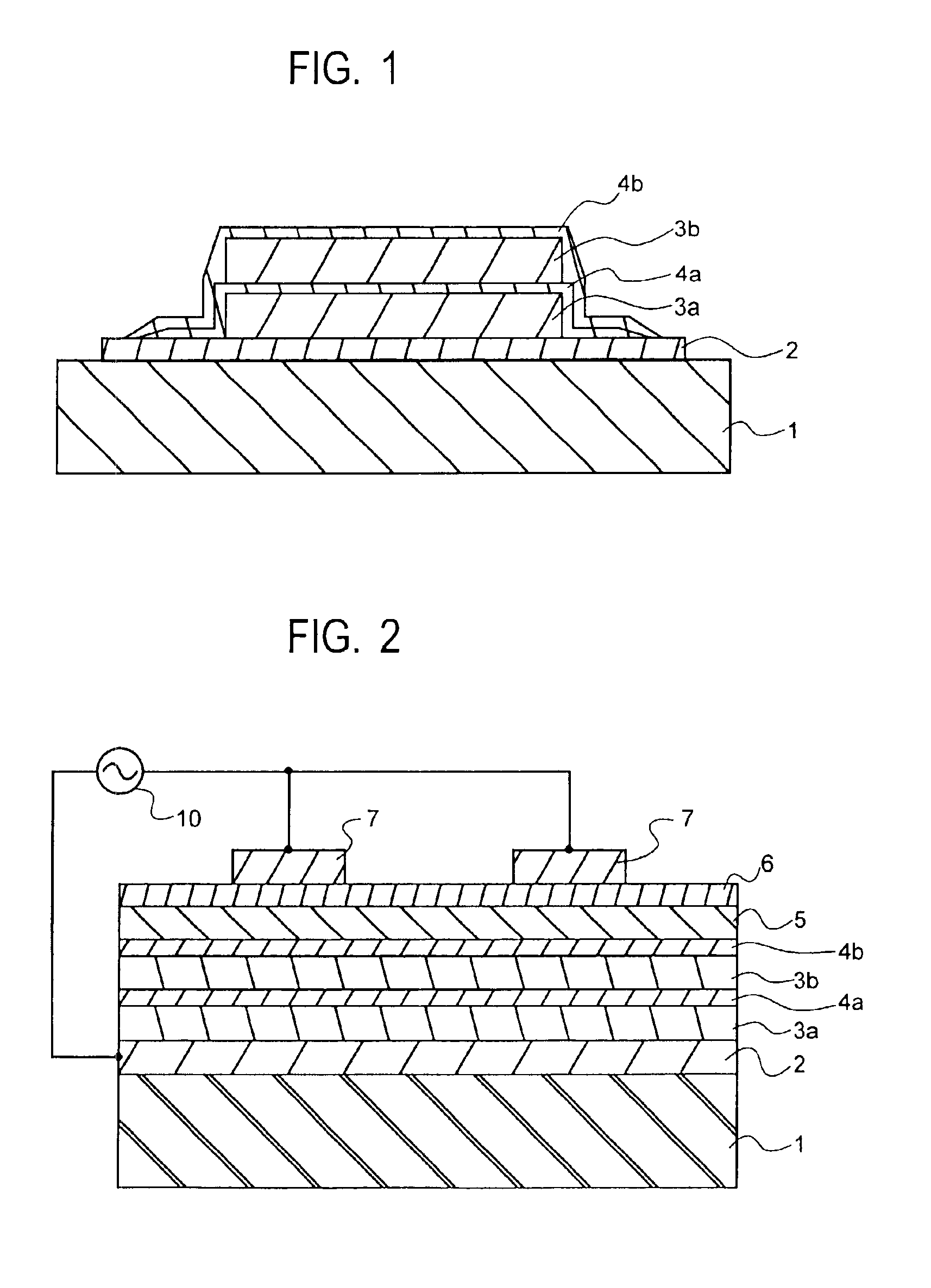
[0114]To conduct a withstand voltage test on composite substrates according to the invention, samples of the construction: alumina substrate / lower Au electrode / composite thick-film dielectric layer (inventive structure) / upper ITO electrode were prepared.
[0115]The lower Au electrode and the upper ITO electrode had the same shape as in Example A-1 and included 80 lines and 70 lines, respectively.
[0116]The composite thick-film dielectric layer was formed by alternately stacking thick-film dielectric layers A and dielectric layers B arising from the solution coating-and-firing technique. The order of stacking is described from left to right.[0117]V-1 sample: A (5 μm) / B (1 μm) / A (10 μm) / B (1 μm)[0118]V-2 sample: B (0.3 μm) / A (5 μm) / B (0.1 μm) / A (10 μm) / B (1 μm)[0119]V-3 sample: A (5 μm) / B (0.1 μm) / A (5 μm) / B (0.1 μm) / A (5 μm) / B (1 μm)
[0120]For comparison with the foregoing samples, a comparative sample V-4 of a conventional structure was prepared.[0121]V-4 sample: A (20 μm) / B (1 μm)
[0122...
PUM
| Property | Measurement | Unit |
|---|---|---|
| thickness | aaaaa | aaaaa |
| width | aaaaa | aaaaa |
| width | aaaaa | aaaaa |
Abstract
Description
Claims
Application Information


