
Raw silicon crusher

a technology of raw silicon and crusher, which is applied in the field of raw silicon crusher, can solve the problems of difficult to avoid the decrease in lower purity of raw silicon, so as to achieve low “loss” and reduce the purity of raw silicon. the effect of power

Inactive Publication Date: 2013-01-15
CHOSHU IND
View PDF5 Cites 0 Cited by
  • Summary
  • Abstract
  • Description
  • Claims
  • Application Information

AI Technical Summary

Benefits of technology

The present invention allows for the crushing of raw silicon with less effort and a higher purity level. By only allowing pure silicon and purified water to touch the raw silicon, the crusher requires less force to achieve the desired result. This leads to a reduction in energy usage and prevents contamination, resulting in a higher quality product.

Problems solved by technology

Even if any raw silicon crush arts are selected, the fineness of the raw silicon decreases, because the tungsten (from the hammers) or the tungsten carbide (from the jaw crusher) contaminates a surface of the raw silicon.
But this method requires the same or more effort to crush it, so workers might hurt their joints and hands.
Because the fitting causes metal contamination, it is difficult to avoid the decrease in purity of the raw silicon.

Method used


Image

  • Raw silicon crusher
  • Raw silicon crusher
  • Raw silicon crusher

Examples


first embodiment

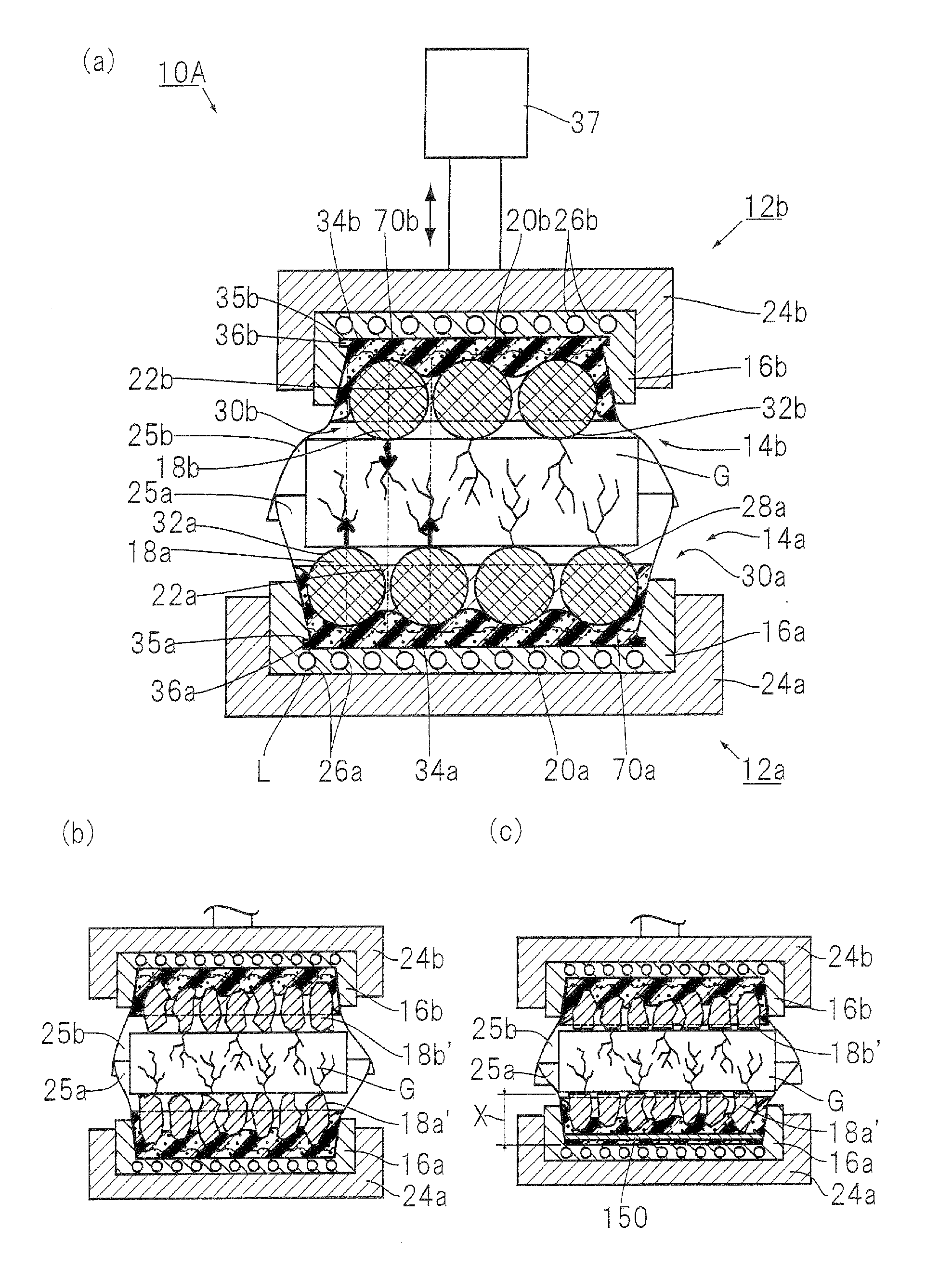
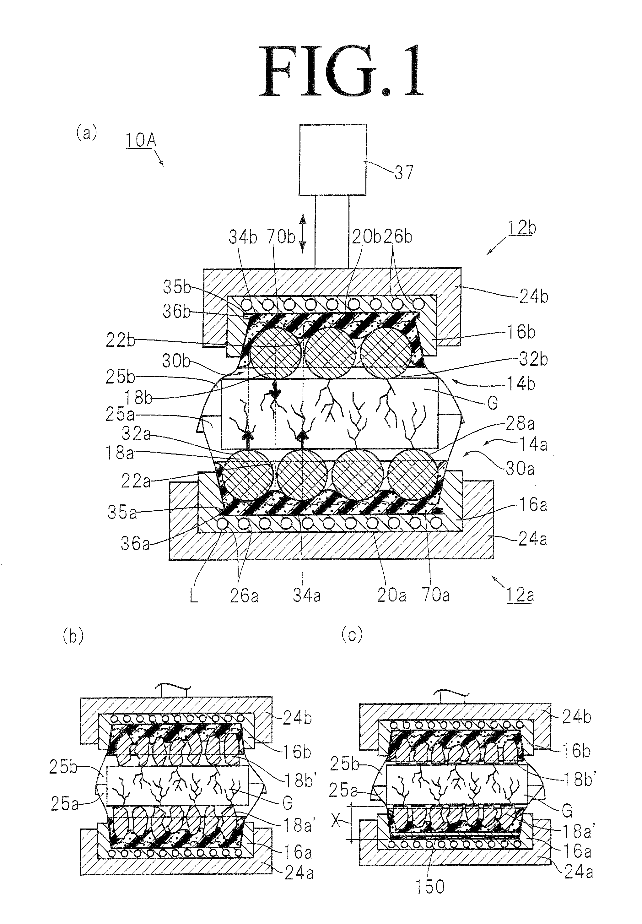
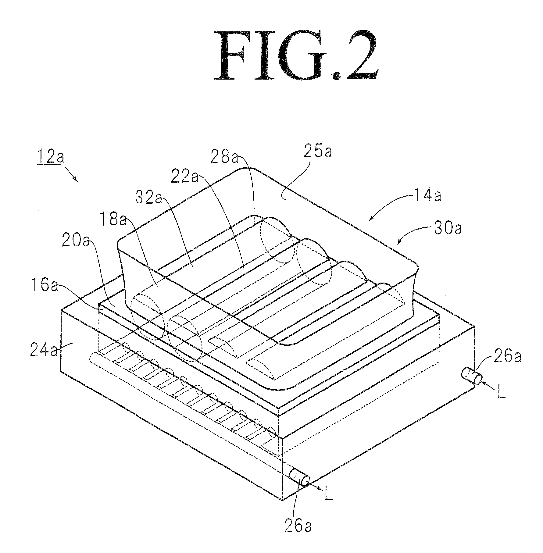
[0050]The raw silicon crusher 10A according to the first embodiment is suitable for crushing quenched and rod-shaped raw silicon G. The crusher 10A is also suitable for remains of the raw silicon made by CZ method, FZ method, or Casting method. As shown in FIG. 1 (a), the raw silicon crusher 10A has a pair of beds 12a, 12b arranged as one above the other. The raw silicon G is crushed by applying pressure between a pair of crushing surfaces 14a, 14b, facing each other, on the beds 12a, 12b. FIG. 2 is a perspective view showing the lower bed 12a. FIG. 1 (a) and FIG. 2 are used for following explanation.

[0051]Each of the beds 12a, 12b has a case 16, non-quenched pure silicon members 18, a foam resin mat 20, a block of ice 22, a base 24, a skirt 25, and a net 70. The base 24, the skirt 25, and the net 70 are not essential parts for the raw silicon crusher 10A.

[0052]The lower bed 12a is explained as follows. The explanation for the lower bed 12a is the same as for the upper bed 12b. Acco...

second embodiment

(Second Embodiment)

[0081]The raw silicon crusher 10B, shown in FIG. 5, according to the second embodiment is suitable for crushing raw silicon G in lump obtained by quenching once (or more) rod-shaped (or block-shaped, irregular-shaped) raw silicon G. The raw silicon crusher 10B has a pair of beds 12c, 12d as well as the first embodiment. The raw silicon G is crushed by applying pressure between a pair of crushing surfaces 14c 14d, facing each other, on the beds 12a, 12b.

[0082]Unlike the first embodiment, irregular-shaped pure silicon members in lump 18c, 18d are used in this embodiment. Additionally, the irregular-shaped pure silicon members in lump 18c, 18d in FIG. 5 are arranged as they stuck out from surfaces of the ice 22c, 22d like tusks as well as the embodiment in FIG. 1 (b). After forming the top of the irregular-shaped pure silicon members 18c, 18d in flat as well as the embodiment in FIG. 1 (c), the flat-top of the irregular-shaped pure silicon members in lump 18c, 18d m...

third embodiment

(Third Embodiment)

[0091]The raw silicon crushing system 100 (as shown in FIG. 6) according to the third embodiment crushes the rod-shape raw silicon G in two stages to “a ball for baseball” or “a peanut” size by combining in series the raw silicon crushers of the first and the second embodiment.

[0092]The raw silicon crushing system 100 has a step-like stage 50 having an upper stage 50a and a lower stage 50b. And the raw silicon crusher 10A and 10B, a chute 102, and a raw silicon washer 104 are provided on the upper and lower stage 50a, 50b. The flat-top irregular shape pure silicon members 18c, 18d may be provided.

[0093]The raw silicon crusher 10A, as described above, is provided on the upper stage 50a. For operating the raw silicon crushing system 100, an upper bed traverse device 106 and a lower bed tilting device 108 also be provided.

[0094]The upper bed 12b of the raw silicon crusher 10A spaced apart the raw silicon G is traversed with the upper bed traverse device 106. The upper...


PUM

PropertyMeasurementUnit
particle sizeaaaaaaaaaa
thicknessaaaaaaaaaa
pressureaaaaaaaaaa

Abstract

The raw silicon crusher comprises a pair of beds; and a pair of crushing surfaces on the beds crushing the quenched pure raw silicon by applying pressure; wherein each of the beds comprises a case; pure silicon members arranged inside of the case and protruding from the opening; a block of pure ice fixing the pure silicon members to the case, and each of the crushing surfaces comprises surfaces of ends of protrusions; and surface of the block of ice.

Description

[0001]This is a 371 of PCT / JP2009 / 003983 Aug. 20, 2009 which is incorporated herein by reference.BACKGROUND OF THE INVENTION[0002]1. Field of the Invention[0003]The present invention relates to a raw silicon crusher that crushes raw silicon for silicon wafers used for semiconductors.[0004]2. Description of the Related Art[0005]Silicon wafers used for semiconductors are produced by cutting radially single crystal silicon rods by predetermined size in thickness. The single crystal silicon rods are produced by “Czochralski process.” The Czochralski process is a method of crystal growth by dipping seed crystal, mounted on a rod, into molten raw silicon before pulling upwards and rotating the rod at a same time. The raw silicon is leftover single crystal silicon after cutting out the silicon wafers, or multicrystal silicon produced by “Siemens process” or “Monosilane process,” for example.[0006]The raw silicon is melted by heat in a silica (quartz) crucible. For efficient melting, the ra...

Claims


Application Information

Patent Timeline
Patent Type & Authority Patents(United States)
IPC IPC(8): B02C1/10
CPCB02C1/005B02C1/04B02C1/046C01B33/02B01J19/18B02C19/18
Inventor MURAI, TSUYOSHIKONAKA, TOSHINORI
Owner CHOSHU IND
Learn More