Method and structure of integrated micro electro-mechanical systems and electronic devices using edge bond pads

a technology of edge bonding and electromechanical system, applied in the direction of semiconductor devices, semiconductor/solid-state device details, electrical apparatus, etc., can solve the problems of reducing cost, focusing on mems development, and still having limitations in ics and in particular mems, and achieves a wide range of applicability, high device yield in dies, and convenient use

Active Publication Date: 2013-02-05
MOVELLA INC
View PDF21 Cites 24 Cited by
  • Summary
  • Abstract
  • Description
  • Claims
  • Application Information

AI Technical Summary

Benefits of technology

[0007]According to the present invention, techniques related generally to integrated devices and systems are provided. More particularly, the present invention provides a method for fabricating an integrated electronic device using edge bond pads as well as a device using edge bond pads. More specifically, the present invention provides a method for forming a passivation material and a conduction material overlying one or more integrated micro electro-mechanical systems and electronic devices formed overlying a substrate as well as the resulting device. Merely by way of example, the integrated device can include at least an accelerometer, a gyroscope, a magnetic sensor, a pressure sensor, a microphone, a humidity sensor, a temperature sensor, a chemical sensor, a biosensor, an inertial sensor, and others. Additionally, the other applications include at least a sensor application or applications, system applications, and broadband applications, among others. But it will be recognized that the invention has a much broader range of applicability.
[0008]In a specific embodiment, the present invention provides a method for fabricating an integrated electronic device using edge bond pads as well as a device using edge bond pads device. The method includes providing a substrate having a surface region and forming one or more integrated micro electro-mechanical systems and electronic devices on a first region overlying the surface region. Each of the integrated micro electro-mechanical systems and electronic devices can have one or more contact regions. The first region can also have a first surface region. One or more trench structures can be formed within one or more portions of the first region. A passivation material can be formed overlying the first region and the one or more trench structures. One or more portions of the passivation material can be removed within a vicinity of one or more of the contact regions. A conduction material can be formed overlying the passivation material, the one or more trench structures, and one or more of the contact regions. One or more portions of the conduction material can be removed within a vicinity of one or more of the contact regions to form one or more bond pad structures. The resulting device can then be singulated within a vicinity of the one or more bond pad structures to form two or more integrated micro electro-mechanical systems and electronic devices having edge bond pads.
[0009]In a specific embodiment, the device includes a substrate having a surface region and one or more integrated micro electro-mechanical systems and electronic devices on a first region overlying the surface region. Each of the integrated micro electro-mechanical systems and electronic devices can have one or more contact regions. The first region can also have a first surface region. The device can also have one or more trench structures within one or more portions of the first region. The device can have a passivation material overlying the first region and the one or more trench structures. The passivation material can have one or more portions removed within a vicinity of one or more of the contact regions. The device can have a conduction material overlying the passivation material, the one or more trench structures, and one or more of the contact regions. The device can also have one or more portions of the conduction material removed within a vicinity of one or more of the contact regions to form one or more bond pad structures. The device can also have one or more edge bond pad structures within a vicinity of the one or more bond pad structures. The one or more edge bond pad structures can be formed by a singulation process within a vicinity of the one or more bond pad structures.
[0010]Many benefits are achieved by way of the present invention over conventional techniques. For example, the present technique provides an easy to use process that relies upon conventional technology. In some embodiments, the method provides higher device yields in dies per wafer with the integrated approach or provides for easier integration of a fabricated device with other devices. Additionally, the method provides a process and system that are compatible with conventional process technology without substantial modifications to conventional equipment and processes. Preferably, the invention provides for an improved MEMS device system and related applications for a variety of uses. In one or more embodiments, the present invention provides for all MEMS and related applications, which may be integrated on one or more CMOS device structures. Depending upon the embodiment, one or more of these benefits may be achieved. These and other benefits will be described in more throughout the present specification and more particularly below.
[0011]Various additional objects, features and advantages of the present invention can be more fully appreciated with reference to the detailed description and accompanying drawings that follow

Problems solved by technology

Although highly successful, ICs and in particular MEMS still have limitations.
Similar to IC development, MEMS development, which focuses on increasing performance, reducing size, and decreasing cost, continues to be challenging.
Additionally, applications of MEMS often require increasingly complex microsystems that desire greater computational power.
Unfortunately, such applications generally do not exist.

Method used


Image

  • Method and structure of integrated micro electro-mechanical systems and electronic devices using edge bond pads
  • Method and structure of integrated micro electro-mechanical systems and electronic devices using edge bond pads
  • Method and structure of integrated micro electro-mechanical systems and electronic devices using edge bond pads

Examples


Embodiment Construction

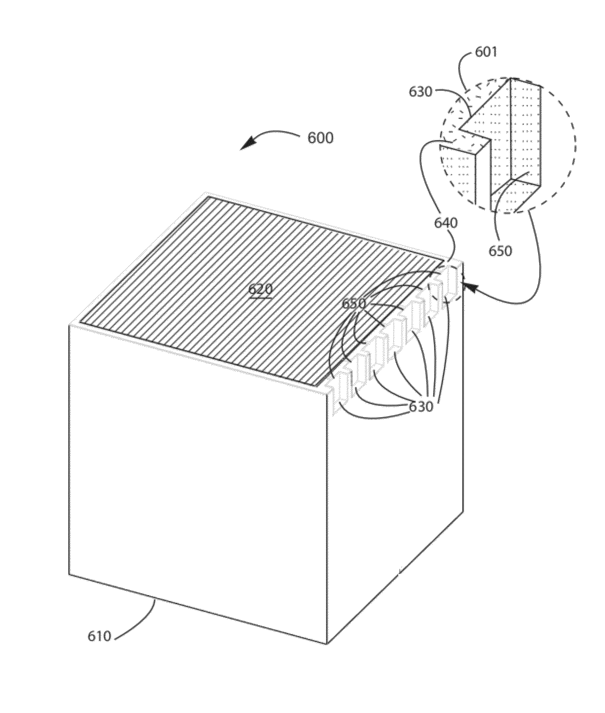
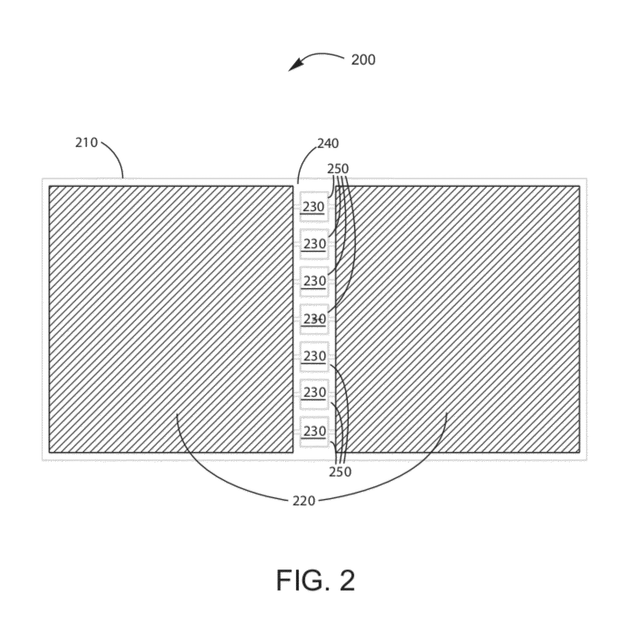
[0018]According to the present invention, techniques related generally to integrated devices and systems are provided. More particularly, the present invention provides a method for fabricating an integrated electronic device using edge bond pads. More specifically, the present invention provides a method for patterning one or more semiconductor layers to form one or more air dielectric regions within an integrated CMOS and MEMS device. Merely by way of example, the MEMS devices can include at least an accelerometer, a gyroscope, a magnetic sensor, a pressure sensor, a microphone, a humidity sensor, a temperature sensor, a chemical sensor, a biosensor, an inertial sensor, and others. Additionally, the other applications include at least a sensor application or applications, system applications, and broadband applications, among others. But it will be recognized that the invention has a much broader range of applicability.

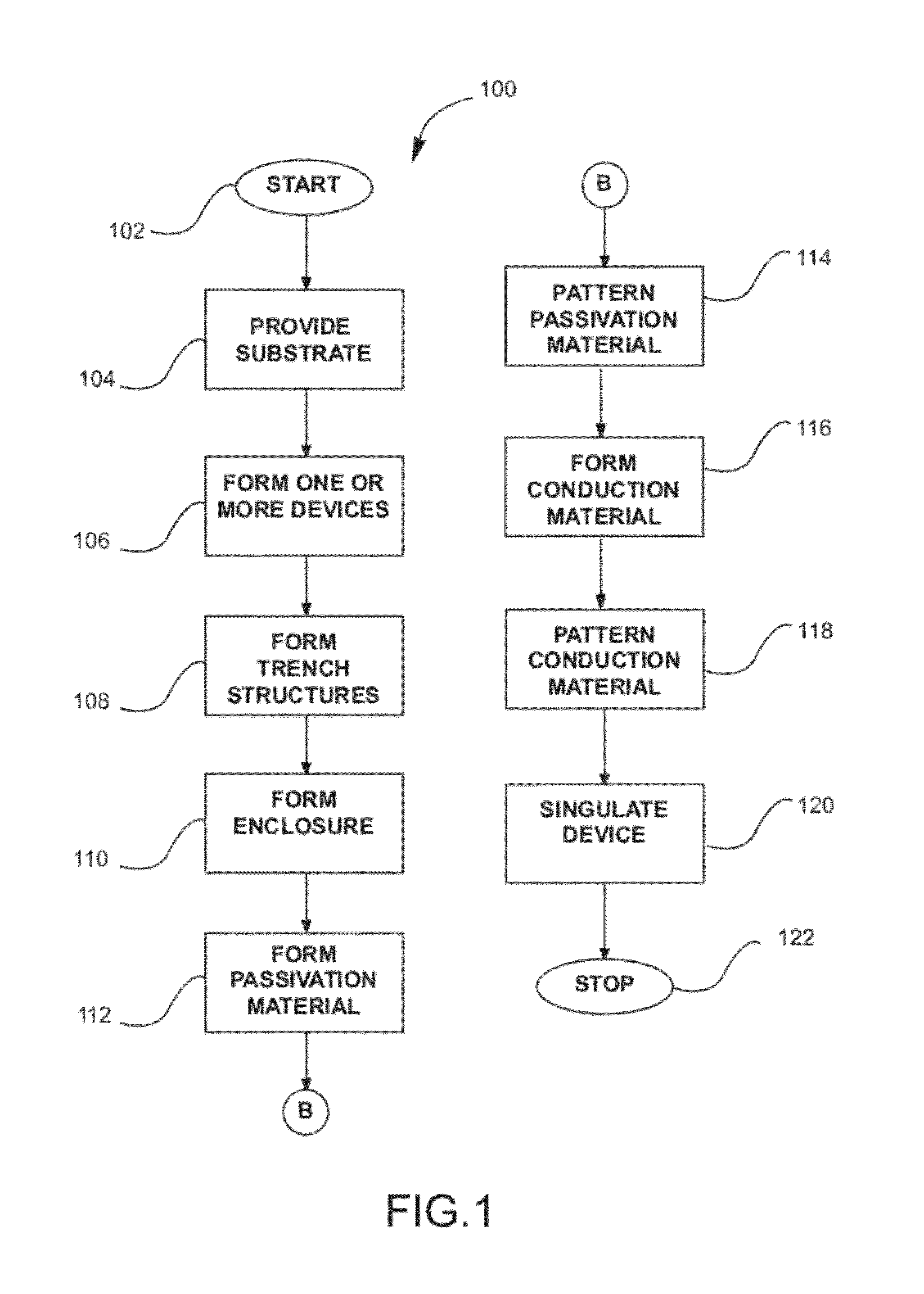
[0019]FIG. 1 is a simplified flow diagram illustrating a metho...


PUM


Abstract

A method for fabricating a monolithic integrated electronic device using edge bond pads as well as the resulting device. The method includes providing a substrate having a surface region and forming one or more integrated micro electro-mechanical systems and electronic devices on a first region overlying the surface region. One or more trench structures can be formed within one or more portions of the first region. A passivation material and a conduction material can be formed overlying the first region and the one or more trench structures. The passivation material and the conduction material can be etched to form one or more bonding pad structure. The resulting device can then be singulated within a vicinity of the one or more bond pad structures to form two or more integrated micro electro-mechanical systems and electronic devices having edge bond pads.

Description

CROSS-REFERENCES TO RELATED APPLICATIONS[0001]The present application claims priority to and incorporates by reference, for all purposes, the following pending patent application: U.S. Pat. App. No. 61 / 322,198, filed Apr. 8, 2010. The present invention also incorporates by reference, for all purposes, the following co-pending patent applications: U.S. patent application Ser. No. 12 / 859,631, filed Aug. 19, 2010, U.S. patent application Ser. No. 12 / 490,067, filed Jun. 23, 2009, U.S. patent application Ser. No. 12 / 945,087, filed Nov. 12, 2010, and U.S. patent application Ser. No. 12 / 913,440, filed Oct. 27, 2010.BACKGROUND OF THE INVENTION[0002]The present invention relates generally to integrated devices. More particularly, the present invention provides a method for fabricating an integrated electronic device using edge bond pads as well as a device using edge bond pads. More specifically, the present invention provides a method for forming a passivation material and a conduction mate...

Claims


Application Information

Patent Timeline
Patent Type & Authority Patents(United States)
IPC IPC(8): H01L21/00
CPCB81C1/00246B81B2207/015B81B2207/098H01L2224/0556H01L24/03H01L24/05H01L2224/05571H01L2224/056H01L2224/94H01L29/0657H01L2924/1461H01L2924/00014H01L2924/10155H01L2924/12042H01L2924/00012H01L2224/03H01L2924/00H01L2224/05552H01L23/488
Inventor YANG, XIAO “CHARLES”
Owner MOVELLA INC
Why Eureka
Try Eureka