Pulsed plasma high aspect ratio dielectric process

a dielectric process and plasma technology, applied in the direction of fluid pressure measurement, instruments, vacuum gauges, etc., can solve the problems of reducing the effective electron temperature, affecting the etching of high aspect ratio dielectric structures on workpieces, and affecting the etching effect of high aspect ratio dielectric structures

Active Publication Date: 2013-02-26
APPLIED MATERIALS INC
View PDF4 Cites 29 Cited by
  • Summary
  • Abstract
  • Description
  • Claims
  • Application Information

AI Technical Summary

Problems solved by technology

Plasma etching of high aspect ratio dielectric structures on workpieces is hampered by problems of aspect ratio dependent etching, etch stop or twisting of etched features.
Generally, pulsing of the plasma reduces the effective electron temperature.
Unfortunately, the typical dielectric etch process gas chemistries do not form a significant population of negative ions; that is, the number density of electrons far exceeds the number density of negative ions.
Consequently, there are unequal fluxes of oppositely charged ions to the workpiece or wafer, leading to charging of the workpiece structure.
However, that is not a complete solution to the charging problem.
Moreover, it does not address a problem of non-uniform radial distribution of plasma ion density.

Method used


Image

  • Pulsed plasma high aspect ratio dielectric process
  • Pulsed plasma high aspect ratio dielectric process
  • Pulsed plasma high aspect ratio dielectric process

Examples


Embodiment Construction

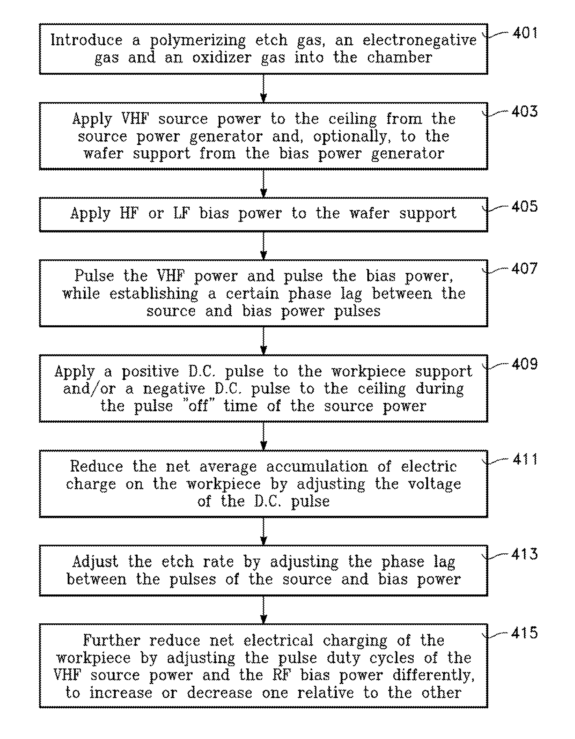
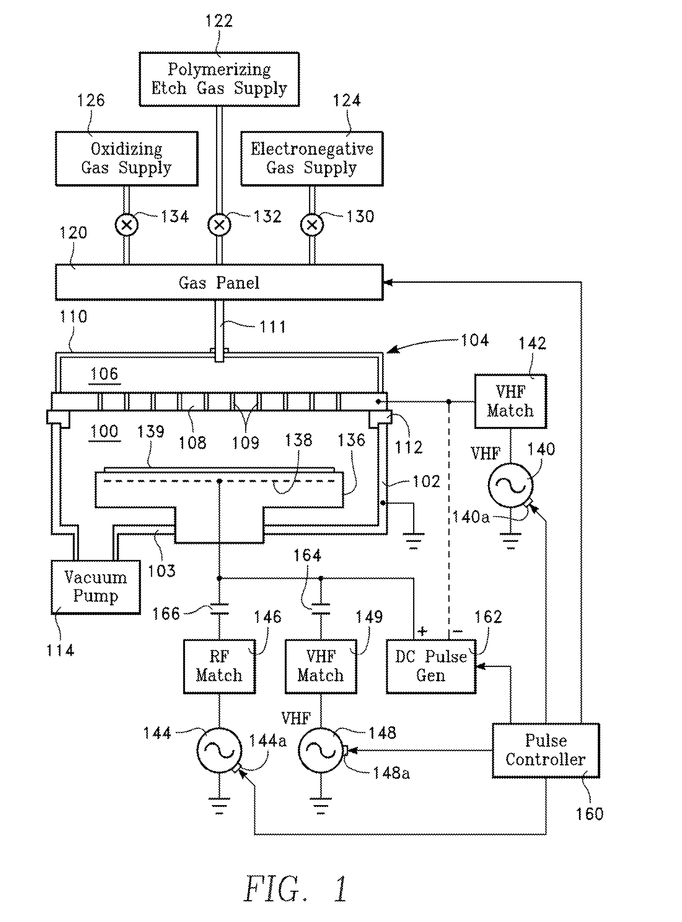
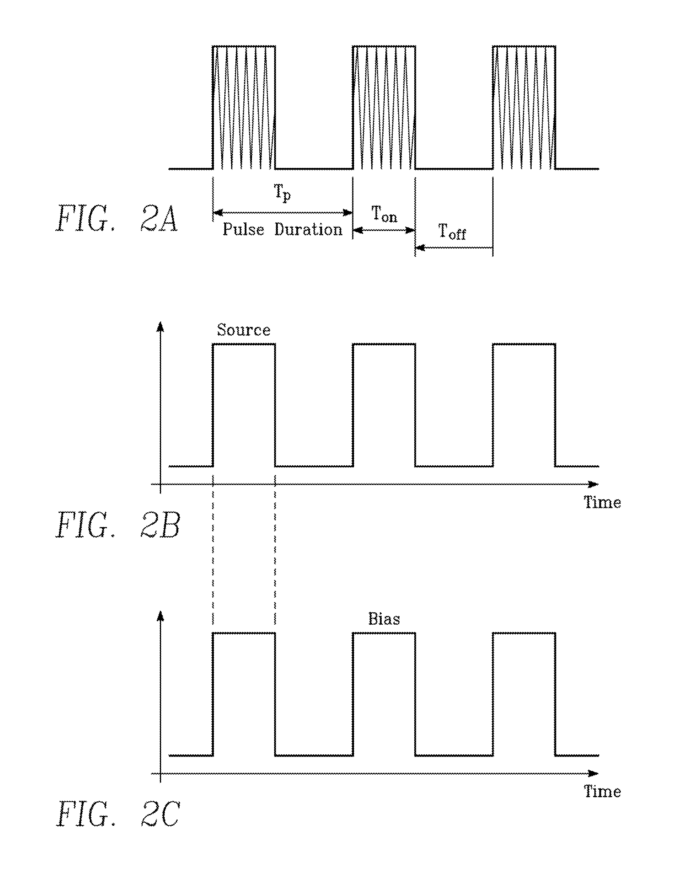
[0019]Uniformity of the radial distribution of plasma ion density is improved in a pulsed RF plasma dielectric etch process. One embodiment uses the phase lead or lag of the RF envelopes of the pulsed RF source power and the pulsed RF bias power to improve uniformity. In this embodiment, VHF source power and HF (and / or MF) bias power are pulsed independently with a phase lead or lag between the source and bias power pulses. The plasma ion distribution responds differently to application of the different frequencies, enabling the ion distribution to be adjusted by adjusting the phase lead or lag. The different distributions attained during the different phases of each cycle average out over a complete cycle to a more uniform distribution. In one embodiment, a combination of a source power frequency in the low region of the VHF range (e.g., 60 MHz) is used in conjunction with a bias power frequency in the HF range (e.g., 13.56 MHz). The bias frequency may produce a predominantly highe...


PUM

PropertyMeasurementUnit
frequencyaaaaaaaaaa
frequencyaaaaaaaaaa
frequencyaaaaaaaaaa

Abstract

Radial distribution of etch rate is controlled by controlling the respective duty cycles of pulsed VHF source power applied to the ceiling and pulsed HF or MF bias power on the workpiece. Net average electrical charging of the workpiece is controlled by providing an electronegative process gas and controlling the voltage of a positive DC pulse on the workpiece applied during pulse off times of the pulsed VHF source power.

Description

CROSS-REFERENCE TO RELATED APPLICATIONS[0001]This application claims the benefit of U.S. Provisional Application Ser. No. 61 / 211,256, filed Mar. 26, 2009 entitled PULSED PLASMA HIGH ASPECT RATIO DIELECTRIC ETCH PROCESS, by Ankur Agarwal, et al.BACKGROUND[0002]1. Technical Field[0003]Disclosed embodiments concern plasma etch processes employed in etching dielectric layers on a workpiece such as a semiconductor wafer.[0004]2. Background Art[0005]Plasma etching of high aspect ratio dielectric structures on workpieces is hampered by problems of aspect ratio dependent etching, etch stop or twisting of etched features. This is due in part to competing polymer deposition and etch mechanisms using fluorocarbon etch chemistry. It is also due in part to negative charging of the structure walls and positive charging of the structure floor or bottom of the high aspect ratio openings from predominantly positive ion fluxes and unequal electron fluxes down the depth of the structure. There is a ne...

Claims


Application Information

Patent Timeline
Patent Type & Authority Patents(United States)
IPC IPC(8): G01L21/30G01R31/00
CPCH01J37/32091H01J37/32165H01J37/32706H01L21/31116
Inventor AGARWAL, ANKURCOLLINS, KENNETH S.RAUF, SHAHIDRAMASWAMY, KARTIKLILL, THORSTEN B.
Owner APPLIED MATERIALS INC
Why Eureka
Try Eureka