Solid-state imaging device including arrays of optical elements and photosensitive cells

a solid-state imaging and array technology, applied in the field of solid-state imaging device sensitivity increase, can solve the problems of decreasing optical efficiency, reducing optical efficiency by color filters, and reducing optical efficiency by color filters, and achieve the effect of high optical efficiency and high optical efficiency

Active Publication Date: 2013-02-26
SAMSUNG ELECTRONICS CO LTD
View PDF25 Cites 25 Cited by
  • Summary
  • Abstract
  • Description
  • Claims
  • Application Information

AI Technical Summary

Benefits of technology

[0062]A solid-state imaging device according to the present invention uses an array of optical elements with a light-splitting function (i.e., light-splitting elements), and therefore, does not need a color filter that absorbs light. As a result, higher optical efficiency is achieved. In addition, since at least two different types of light-splitting elements are used, at least two kinds of color components can be obtained from the photosensitive cells. If the signals supplied from multiple photosensitive cells are appropriately added together, a white component can be obtained. And by subtracting those two kinds of color components from the white component, another kind of color component can be produced. Consequently, if two types of light-splitting elements are used, high optical efficiency can be achieved and at least three different kinds of color signals that are needed to get color separation done can be obtained.

Problems solved by technology

A normal color filter transmits one color component of incoming light but absorbs the other components of the light, thus decreasing the optical efficiency.
Specifically, in a color camera that uses a Bayer color filter, for example, a subtractive color filter that uses an organic pigment as a dye is arranged over each photosensing section of an imager, and therefore, the optical efficiency achieved is rather low.
It is true that the aperture ratio can be increased substantially by this technique but the decrease in optical efficiency by color filters still persists.
Nevertheless, even if such a technique is adopted, the optical efficiency cannot be 100%, as one out of the three colors should be sacrificed.
In this case, as light absorbing color elements are used, the RGB light rays cannot be used so efficiently.

Method used


Image

  • Solid-state imaging device including arrays of optical elements and photosensitive cells
  • Solid-state imaging device including arrays of optical elements and photosensitive cells
  • Solid-state imaging device including arrays of optical elements and photosensitive cells

Examples


embodiment 1

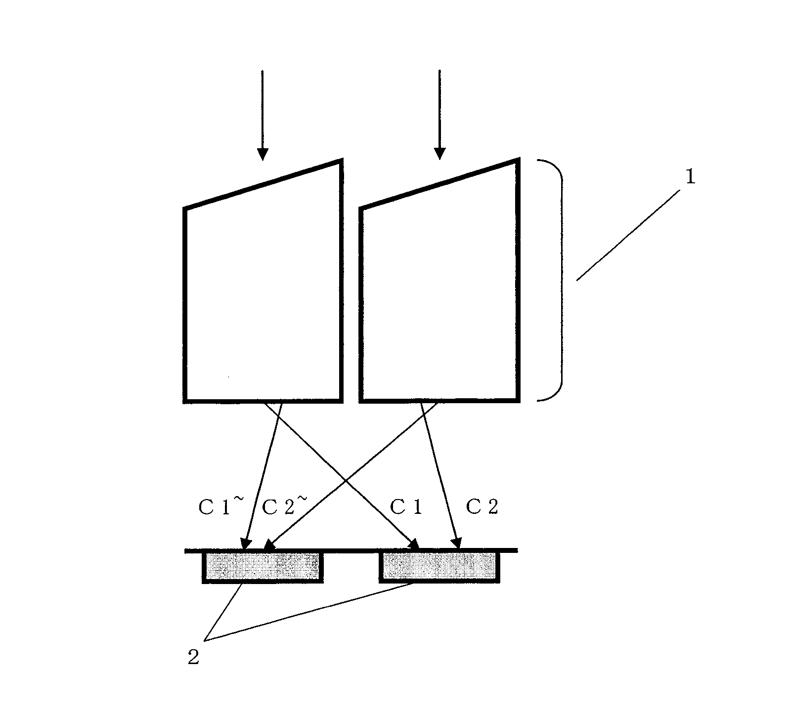
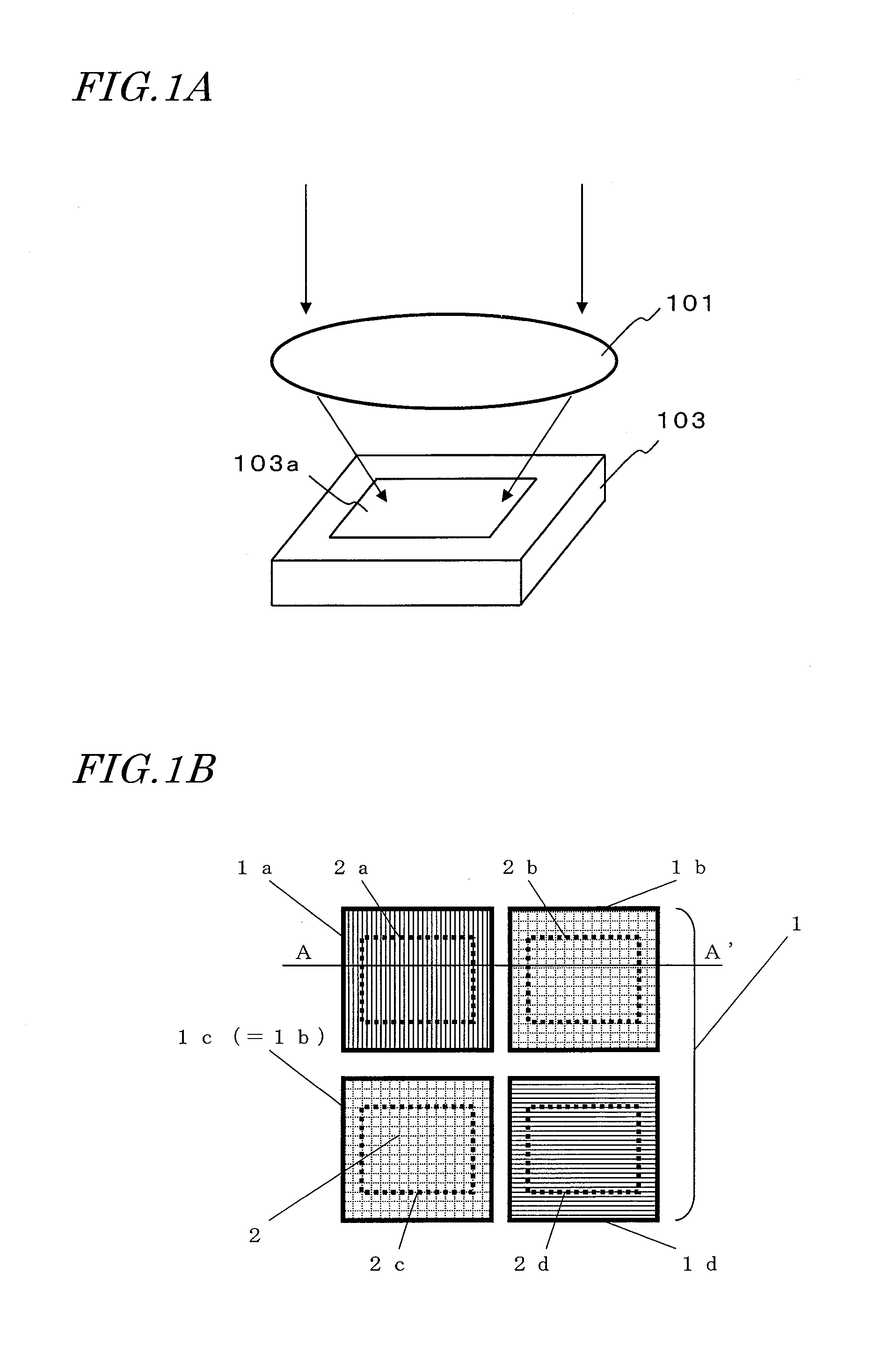
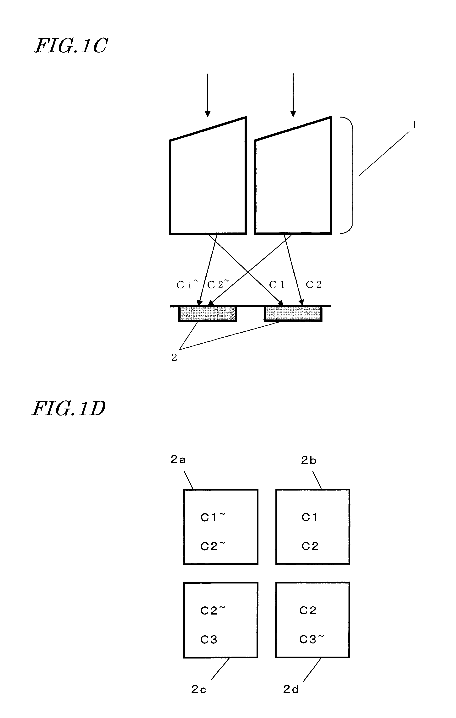
[0129]FIG. 1a is a perspective view illustrating how light that has been transmitted through a lens 101 is incident on a solid-state imaging device 103. On the imaging plane 103a of the solid-state imaging device 103, arranged two-dimensionally are a lot of photosensitive cells. Since the light is imaged by the lens 101, the intensity of the light falling on the imaging plane 103a (which will be referred to herein as an “incident light intensity”) varies according to the point of incidence. Those photosensitive cells are typically photodiodes, each of which outputs an electrical signal representing the incident light intensity by photoelectric conversion (such a signal will be referred to herein as a “photoelectrically converted signal”). The solid-state imaging device 103 is typically implemented as a CCD or a CMOS sensor and is fabricated by known semiconductor device processing. In the solid-state imaging device 103 of this preferred embodiment, an array of optical elements with ...

embodiment 2

[0145]Hereinafter, a second preferred embodiment of the present invention will be described with reference to the accompanying drawings. FIG. 2A is a plan view illustrating the arrangement of an array of optical elements according to this second preferred embodiment of the present invention in an imager that uses a 2 by 2 matrix of photosensitive cells as its fundamental unit. FIG. 2B is a plan view illustrating the kinds of light rays to be incident on those photosensitive cells.

[0146]The fundamental unit of this preferred embodiment is similar to that of the first preferred embodiment described above but is different from its counterpart in that an element associated with the light-splitting element 1d in the array of optical elements is a transparent element 1e, not the photosensitive cell.

[0147]The light-splitting elements 1a and b of this preferred embodiment are the same as their counterparts 1a and 1b of the first preferred embodiment described above. That is why the photosen...

embodiment 3

[0150]Hereinafter, a third preferred embodiment of the present invention will be described with reference to the accompanying drawings. FIG. 3 is a plan view illustrating the arrangement of an array of optical elements according to this third preferred embodiment of the present invention in an imager that uses a 2 by 2 matrix of photosensitive cells as its fundamental unit. FIG. 3B is a plan view illustrating the kinds of light rays to be incident on those photosensitive cells.

[0151]The fundamental unit of the array of optical elements of this preferred embodiment is similar to that of the first preferred embodiment described above but is different from its counterpart in that elements associated with the light-splitting element 1b and 1c in the array of optical elements are transparent elements 1e. But other than that, the fundamental unit of this preferred embodiment is quite the same as that of the first preferred embodiment. That is to say, in the 2 by 2 fundamental cell unit, o...


PUM


Abstract

Light-splitting elements are arranged in at least two columns and two rows to form two pairs 1a, 1b and 1c, 1d. Each element splits incident light into light rays and makes them fall on a portion of a photosensing section right under itself and an adjacent photosensitive cell. The element 1a splits the incident light so that a primary color ray C1 and its complementary color ray C1′ enter an adjacent cell 2b and an underlying cell 2a, respectively. The element 1b makes a primary color ray C2 and its complementary color ray C2′ enter an underlying cell 2a and an adjacent cell 2a, respectively. The element 1c does the same as the element 1b. And the element 1d makes a primary color ray C3 and its complementary color ray C3′ enter an adjacent cell 2c and an underlying cell 2d, respectively. These photosensitive cells 2 perform photoelectric conversion, thereby outputting an electrical signal representing the intensity of the incident light. By carrying out simple calculations between the outputs of these cells, a color signal and a luminance signal are generated.

Description

TECHNICAL FIELD[0001]The present invention relates to a technique for increasing the sensitivity of a solid-state imaging device and a technique for realizing color representation using an infrared ray for such a device.BACKGROUND ART[0002]Recently, the performance and functionality digital cameras and digital movie cameras that use some solid-state imaging device such as a CCD and a CMOS (which will be sometimes referred to herein as an “imager”) have been enhanced to an astonishing degree. In particular, the size of a pixel structure for use in a solid-state imaging device has been further reduced these days thanks to development of semiconductor device processing technologies, thus getting an even greater number of pixels and drivers integrated together in a solid-state imaging device. As a result, the resolution of an imager has lately increased significantly from one million pixels to ten million pixels in a matter of few years. Meanwhile, the greater the number of pixels in an...

Claims


Application Information

Patent Timeline
Patent Type & Authority Patents(United States)
IPC IPC(8): H04N3/14H04N5/335H04N9/04H04N9/07H04N5/225
CPCH01L27/14621H01L27/14629H04N5/33H04N9/045H04N5/2254H01L27/14627H01L27/14625H04N25/134
Inventor HIRAMOTO, MASAOYONEMOTO, KAZUYANISHIWAKI, SEIJISUZUKI, MASAAKISUGITANI, YOSHIAKIWAKABAYASHI, SHINICHI
Owner SAMSUNG ELECTRONICS CO LTD
Why Eureka
Try Eureka