Semiconductor optical modulation device, Mach-Zehnder interferometer type semiconductor optical modulator, and method for producing semiconductor optical modulation device

a semiconductor optical modulator and semiconductor technology, applied in optics, instruments, electrical equipment, etc., can solve the problems of requiring a long time period, achieve the effect of reducing refractive index, increasing bandgap energy, and increasing resistivity

Inactive Publication Date: 2013-02-26
SUMITOMO ELECTRIC IND LTD
View PDF4 Cites 2 Cited by
  • Summary
  • Abstract
  • Description
  • Claims
  • Application Information

AI Technical Summary

Benefits of technology

[0007]In the semiconductor optical modulation device according to the above aspect, the optical waveguide layer includes the first semiconductor optical confinement layer, the second semiconductor optical confinement layer, and the insulating layer disposed between the first and second semiconductor optical confinement layers. The insulating layer is made of aluminum oxide. Thus, the insulating layer has a larger bandgap energy than the first and second semiconductor cladding layers and the first and second semiconductor optical confinement layers. The insulating layer has a higher resistivity than the first and second semiconductor cladding layers and the first and second semiconductor optical confinement layers. This prevents carriers or current from flowing through the insulating layer.
[0008]Assume that the first conductivity type is n-type and the second conductivity type is p-type. In this semiconductor optical modulation device, if a negative voltage is applied to the first electrode and a positive voltage is applied to the second electrode, carries (in this example, electrons) are injected from the first semiconductor cladding layer (in this example, n-type) to the first semiconductor optical confinement layer. On the other hand, carries (in this example, holes) are injected from the second semiconductor cladding layer (in this example, p-type) to the second semiconductor optical confinement layer. Accordingly, carriers (in this example, electrons) are accumulated in the first semiconductor optical confinement layer, and carriers (in this example, holes) are accumulated in the second semiconductor optical confinement layer. This produces the carrier plasma effect to decrease the refractive index of the first and second semiconductor optical confinement layers.
[0011]In the semiconductor optical modulation device according to the above aspect, the insulating layer may have a thickness of 5 to 50 nm. In addition, the first semiconductor optical confinement layer and the second semiconductor optical confinement layer may each have a thickness of 20 to 100 nm. In addition, the average refractive index nave of the optical waveguide layer constituted by the first semiconductor optical confinement layer, the insulating layer, and the second semiconductor optical confinement layer may be higher than the refractive indices of the first semiconductor cladding layer and the second semiconductor cladding layer. In the semiconductor optical modulation device according to the above aspect, light propagating in the optical waveguide layer can be effectively confined therein.
[0018]In the Mach-Zehnder interferometer type semiconductor optical modulator according to the above aspect, preferably, the two optical input ports and two optical output ports of each of the first and second MMI couplers form a through-port and a cross-port with each other, the first and second MMI couplers are configured to delay the phase of light traveling through the cross-port by 90° and not to shift the phase of light traveling through the through-port, and the first arm has a longer optical path length than the second arm by the length equivalent to a phase delay of 90°. According to the above aspect, a Mach-Zehnder interferometer type semiconductor optical modulator capable of on / off operation can be easily provided.
[0020]In the method for producing a semiconductor optical modulation device according to the above aspect, after the semiconductor region including the first semiconductor optical confinement layer, the group III-V compound semiconductor layer, and the second semiconductor optical confinement layer is formed, the group III-V compound semiconductor layer in the semiconductor region is oxidized. The group III-V compound semiconductor layer, which contains aluminum as a group III element, can be easily oxidized. Thus, the insulating layer can be easily formed between the first semiconductor optical confinement layer and the second semiconductor optical confinement layer.

Problems solved by technology

The disappearance of carriers, however, is determined by the carrier lifetime, which requires a long period of time.

Method used


Image

  • Semiconductor optical modulation device, Mach-Zehnder interferometer type semiconductor optical modulator, and method for producing semiconductor optical modulation device
  • Semiconductor optical modulation device, Mach-Zehnder interferometer type semiconductor optical modulator, and method for producing semiconductor optical modulation device
  • Semiconductor optical modulation device, Mach-Zehnder interferometer type semiconductor optical modulator, and method for producing semiconductor optical modulation device

Examples


Embodiment Construction

[0031]Embodiments of the present invention will now be described in detail with reference to the attached drawings, where like designations denote like elements. An XYZ Cartesian coordinate system S is shown in the drawings where necessary.

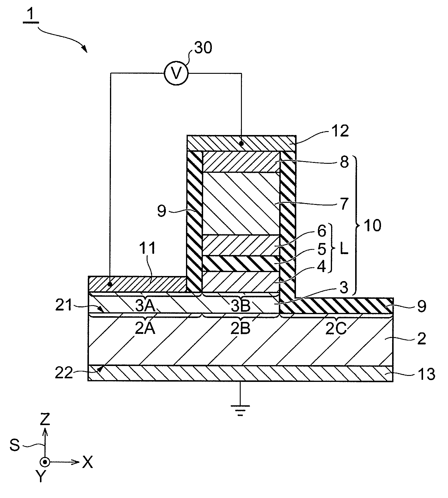
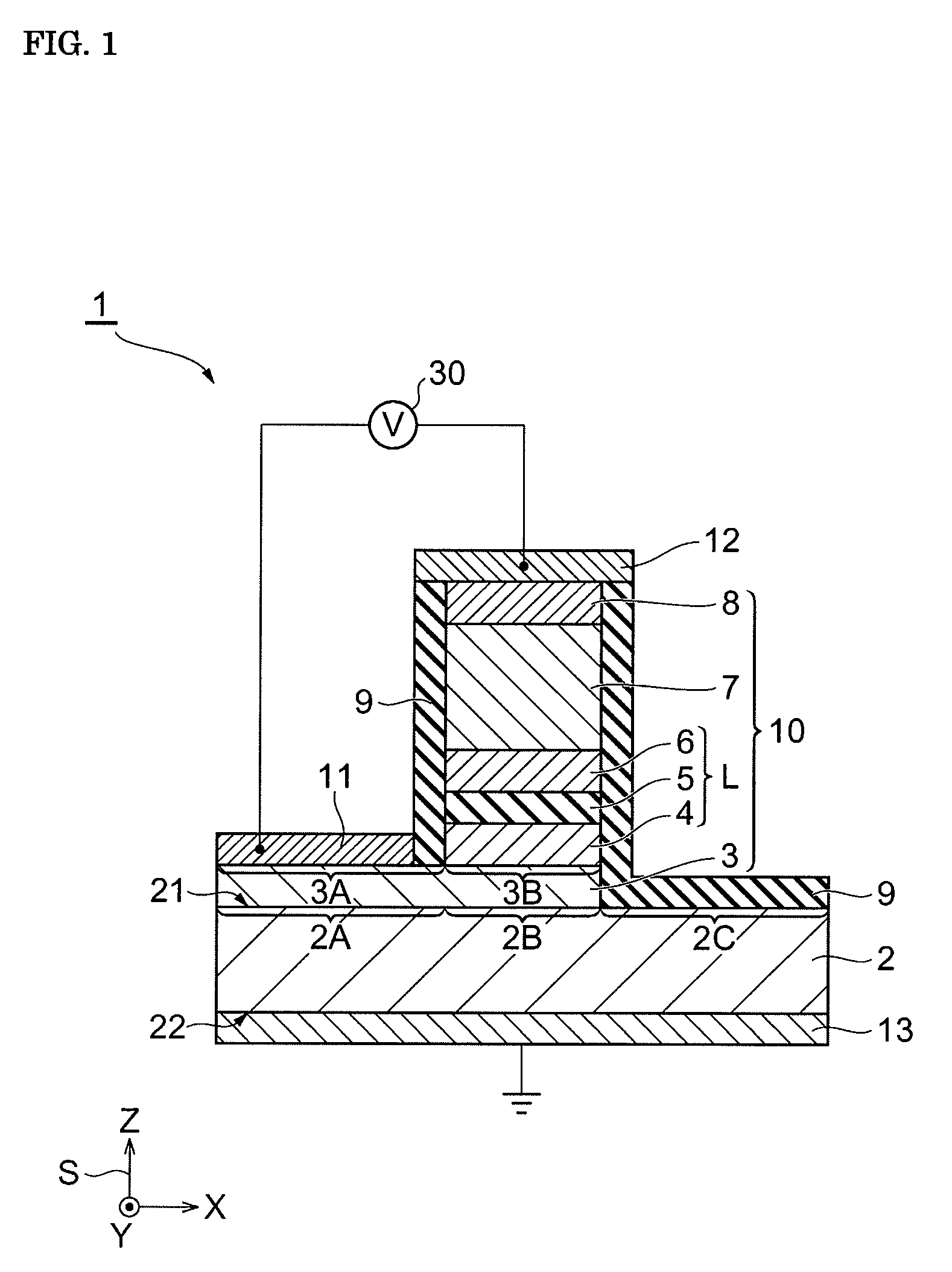
[0032]FIG. 1 is a sectional view of a semiconductor optical modulation device 1 according to an embodiment of the present invention. The semiconductor optical modulation device 1 includes a substrate 2, a first semiconductor cladding layer 3, an optical waveguide layer L, a second semiconductor cladding layer 7, a contact layer 8, a protective film 9, a first electrode 11, a second electrode 12, and a third electrode 13. The optical waveguide layer L includes a first semiconductor optical confinement layer 4, an insulating layer 5, and a second semiconductor optical confinement layer 6. The semiconductor optical modulation device 1 has a semiconductor mesa structure 10 disposed on the substrate 2. This semiconductor mesa structure 10 includes the ...


PUM

PropertyMeasurementUnit
thicknessaaaaaaaaaa
thicknessaaaaaaaaaa
refractive indexaaaaaaaaaa

Abstract

A semiconductor optical modulation device includes a substrate; a first semiconductor cladding layer of a first conductivity type disposed on the substrate; an optical waveguide layer disposed on the first semiconductor cladding layer, the optical waveguide layer including a first semiconductor optical confinement layer, a second semiconductor optical confinement layer, and an insulating layer disposed between the first semiconductor optical confinement layer and the second semiconductor optical confinement layer, the insulating layer being made of aluminum oxide; a second semiconductor cladding layer of a second conductivity type disposed on the optical waveguide layer; a first electrode electrically connected to the first semiconductor cladding layer; and a second electrode electrically connected to the second semiconductor cladding layer.

Description

BACKGROUND OF THE INVENTION[0001]1. Field of the Invention[0002]The present invention relates to semiconductor optical modulation devices, Mach-Zehnder interferometer type semiconductor optical modulators, and methods for producing semiconductor optical modulation devices.[0003]2. Description of the Related Art[0004]PCT International Publication No. WO 2004 / 081638 (Patent Document 1) discloses a semiconductor optical modulator. In this semiconductor optical modulator, the refractive index of a semiconductor layer is changed by applying an electric field to the semiconductor layer using the quantum-confined Stark effect (QCSE) or the Pockels effect. Therefore, optical light is modulated by changing the refractive index of the semiconductor layer according to changing the electric field. Japanese Unexamined Patent Application Publication No. 2008-66318 (Patent Document 2) discloses a semiconductor tunable laser. In this semiconductor tunable laser, the refractive index of a semiconduc...

Claims


Application Information

Patent Timeline
Patent Type & Authority Patents(United States)
IPC IPC(8): G02F1/03
CPCG02F1/025G02F1/2257
Inventor FUKUDA, CHIE
Owner SUMITOMO ELECTRIC IND LTD
Why Eureka
Try Eureka