Semiconductor nanoparticles and method of producing semiconductor nanoparticles

a technology of semiconductor nanoparticles and nanoparticles, which is applied in the field of semiconductor nanoparticles, a method of producing semiconductor nanoparticles, and a light-emitting device, which can solve the problems of high toxicity and unsuitable light-emitting devices

Active Publication Date: 2017-09-21
OSAKA UNIV +2
View PDF6 Cites 18 Cited by
  • Summary
  • Abstract
  • Description
  • Claims
  • Application Information

AI Technical Summary

Benefits of technology

[0009]Therefore, one object of certain embodiments of the present disclosure is to provide semiconductor nanoparticles that are configured to produce band-edge emission from ternary or quaternary quantum dots with a less toxic composition, and a method of producing the semiconductor nanoparticles.
[0014]In the semiconductor nanoparticles according to certain embodiments of the present disclosure, the surface of the core made of a ternary semiconductor is covered with the shell made of the semiconductor containing the Group 13 element and the Group 16 element, the shell having a bandgap energy larger than that of the semiconductor forming the core. With this arrangement, photoluminescence emission with a short photoluminescence lifetime, i.e., the band-edge emission, which cannot be obtained by conventional ternary quantum dots, is obtained. In the semiconductor nanoparticles, each of the core and shell can have composition that contains neither Cd nor Pb, which are highly toxic. Thus, the semiconductor nanoparticles can be applied to products that are prohibited from using Cd or the like. Therefore, such semiconductor nanoparticles are suitable for use as a wavelength conversion material for light-emitting devices used in the liquid crystal display device or the like or as a biomolecule marker. Furthermore, with the method of producing semiconductor nanoparticles as described above, the ternary semiconductor nanoparticles that exhibit band-edge emission can be relatively easily produced.

Problems solved by technology

Such light emission is not suitable for light-emitting devices, particularly, used in liquid crystal display device.
In the semiconductor nanoparticles, each of the core and shell can have composition that contains neither Cd nor Pb, which are highly toxic.

Method used


Image

  • Semiconductor nanoparticles and method of producing semiconductor nanoparticles
  • Semiconductor nanoparticles and method of producing semiconductor nanoparticles
  • Semiconductor nanoparticles and method of producing semiconductor nanoparticles

Examples


example 1

(1) Production of Primary Semiconductor Nanoparticles (Ag—In—S)

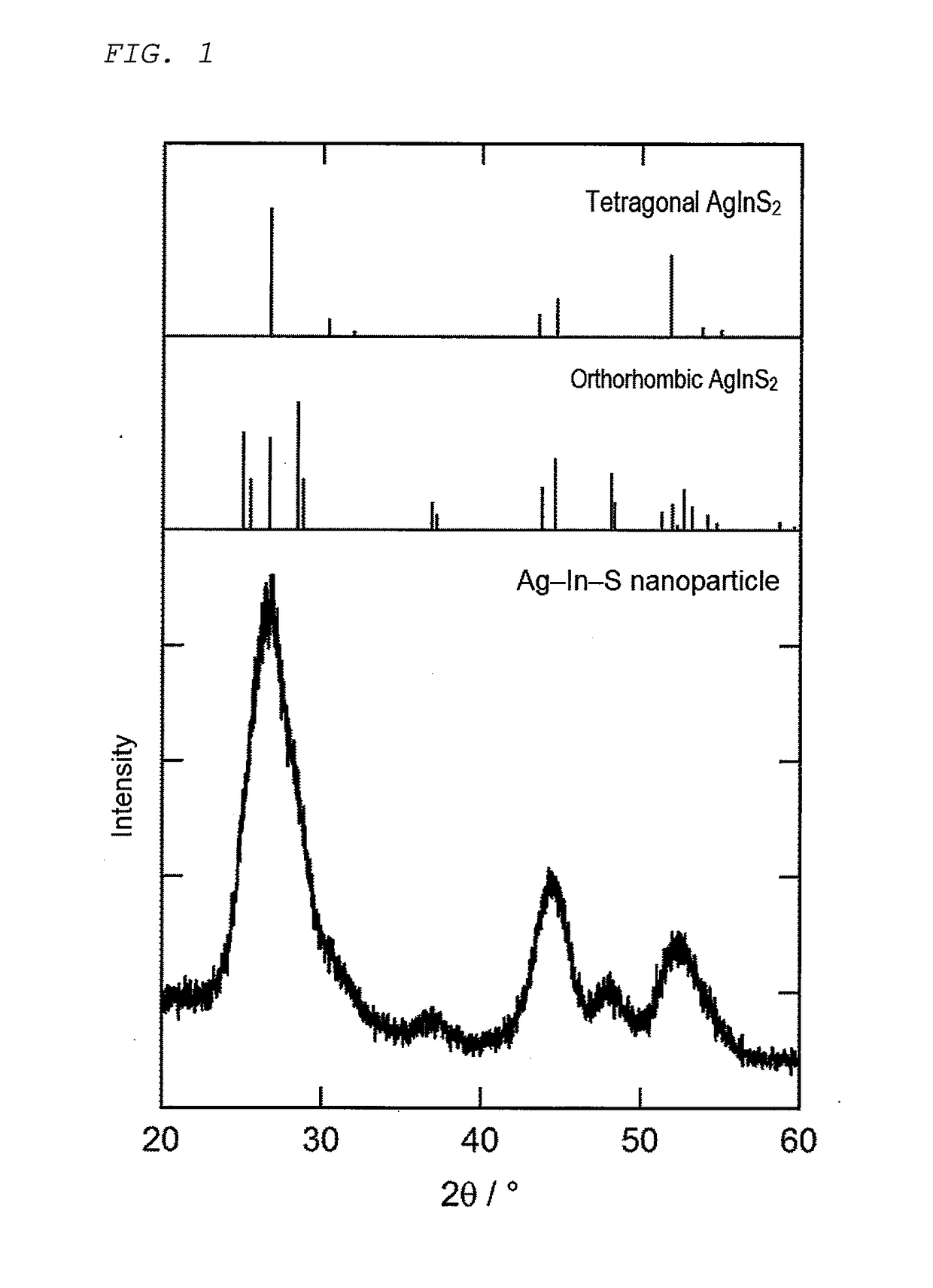
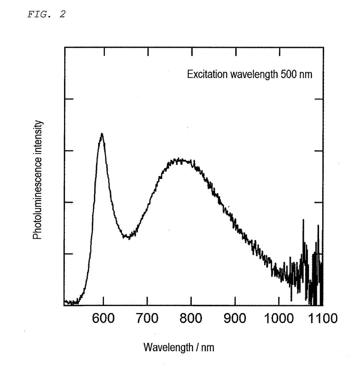
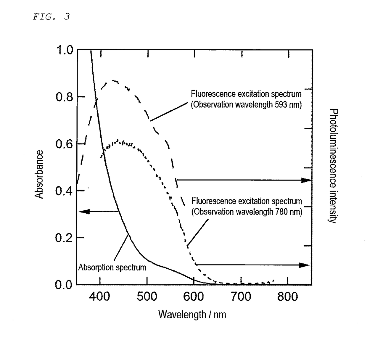
[0129]First, 0.4 mmol of each of silver acetate (AgOAc) and indium acetate (In(OAc)3), 0.8 mmol of thiourea, 11.8 mL of oleylamine, and 0.2 mL of 1-dodecanethiol were charged into a two-necked flask and subjected to vacuum deaeration (for 3 minutes at normal temperature), followed by heating under an Ar atmosphere at a temperature increasing rate of 10° C. / min up to 200° C. The obtained suspension was allowed to cool, followed by centrifugal separation (with a radius of 150 mm at 2,500 rpm for 10 minutes), so that a supernatant dark red liquid was taken out. Then, methanol was added to the supernatant solution until nanoparticles were precipitated, followed by centrifugal separation (with a radius of 150 mm at 2,500 rpm for 3 minutes). Then, the precipitates were dried at the normal temperature under vacuum, thereby producing semiconductor nanoparticles (primary semiconductor nanoparticles).

[0130]An XRD pattern of the ob...

example 2

[0137]First, 10 nmol of the primary semiconductor nanoparticles, obtained in the same procedure as in Example 1, at amount of nanoparticles was dispersed into 12 mL of oleylamine to obtain a dispersion, which was then held at 260° C. under an Ar atmosphere. Separately from this, gallium acetylacetonate (Ga(acac)3) and sulfur powder were added to oleylamine at concentrations of 0.1 mmol / mL and 0.15 mmol / mL, respectively, and then stirred at 100° C. for 10 minutes, so that the gallium acetylacetonate and sulfur powder were dissolved and a mixture was obtained. Then, 4 ml of the mixture was dropped into the above-mentioned heated dispersion at a rate of 5 mL / h (at 0.5 mmol / h based on Ga). When the addition of the mixture is finished, the heating source was turned off, allowing the solution containing the dispersion with the mixture to cool down to the room temperature. Thereafter, methanol was added to the solution, so that precipitates of the core-shell semiconductor nanoparticles is ...

example 3

[0140]First, 30 nmol of the primary semiconductor nanoparticles, obtained in the same procedure as in Example 1, at amount of nanoparticles, 0.1 mmol of gallium acetylacetonate (Ga(acac)3), 0.05 mmol of dibenzyldisulfide and 12 mL of oleylamine were charged into a flask and then heated to 260° C. at a temperature increasing rate of 10° C. / min. After the solution was held at 260° C. for 20 minutes, the heating source was turned off, allowing the solution to cool. Thereafter, methanol was added to the solution, so that precipitates of the core-shell semiconductor nanoparticles is obtained. Then, solid components were collected from the solution by centrifugal separation (with a radius of 150 mm at 2,500 rpm for 3 minutes). The solid components were dissolved into chloroform, and then various properties of the obtained core-shell semiconductor nanoparticles were measured. Upon measuring an average particle size of particles each covered with the shell, the average particle size of the ...


PUM

PropertyMeasurementUnit
full width at half maximumaaaaaaaaaa
temperatureaaaaaaaaaa
particle sizeaaaaaaaaaa

Abstract

A semiconductor nanoparticle includes a core and a shell covering a surface of the core. The shell has a larger bandgap energy than the core and is in heterojunction with the core. The semiconductor nanoparticle emits light when irradiated with light. The core is made of a semiconductor that contains M1, M2, and Z. M1 is at least one element selected from the group consisting of Ag, Cu, and Au. M2 is at least one element selected from the group consisting of Al, Ga, In and Tl. Z is at least one element selected from the group consisting of S, Se, and Te. The shell is made of a semiconductor that consists essentially of a Group 13 element and a Group 16 element.

Description

CROSS REFERENCE TO RELATED APPLICATIONS[0001]This application claims the benefit of Japanese Patent Application Nos. 2016-055299, 2016-177631, and 2017-037487, filed on Mar. 18, 2016, Sep. 12, 2016, and Feb. 28, 2017, respectively. The entire disclosures of Japanese Patent Application Nos. 2016-055299, 2016-177631 and 2017-037487 are hereby incorporated by reference.BACKGROUND[0002]Technical Field[0003]The present disclosure relates to semiconductor nanoparticles, a method of producing the semiconductor nanoparticles, and a light-emitting device using the semiconductor nanoparticles.[0004]Description of Related Art[0005]White light-emitting devices, which are used as backlights of a liquid crystal display devices and the like and which utilize photoluminescence emission from quantum dots (also called “semiconductor quantum dots”), have been proposed. Fine particles of semiconductor with a particle size of 10 nm or less, for example, are known to exhibit a quantum size effect. Such n...

Claims


Application Information

Patent Timeline
Patent Type & Authority Applications(United States)
IPC IPC(8): C09K11/62H01L33/50G02F1/1335B01J13/02
CPCC09K11/621B01J13/02H01L33/502G02F1/133617B82Y30/00B82Y40/00G02F2001/133614Y10S977/813Y10S977/896Y10S977/892Y10S977/95H01L2933/0083Y10S977/774C09K11/02C09B67/0097G02F1/133614
Inventor KUWABATA, SUSUMUUEMATSU, TAROWAJIMA, KAZUTAKATORIMOTO, TSUKASAKAMEYAMA, TATSUYAOYAMATSU, DAISUKENIKI, KENTA
Owner OSAKA UNIV
Why Eureka
Try Eureka