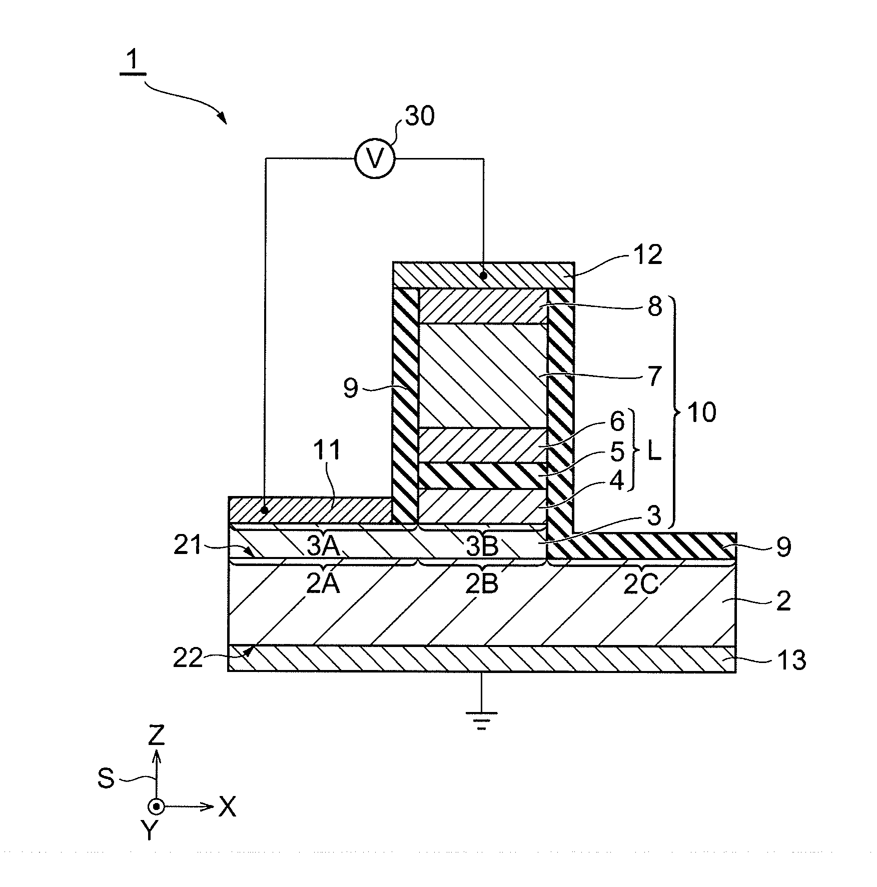
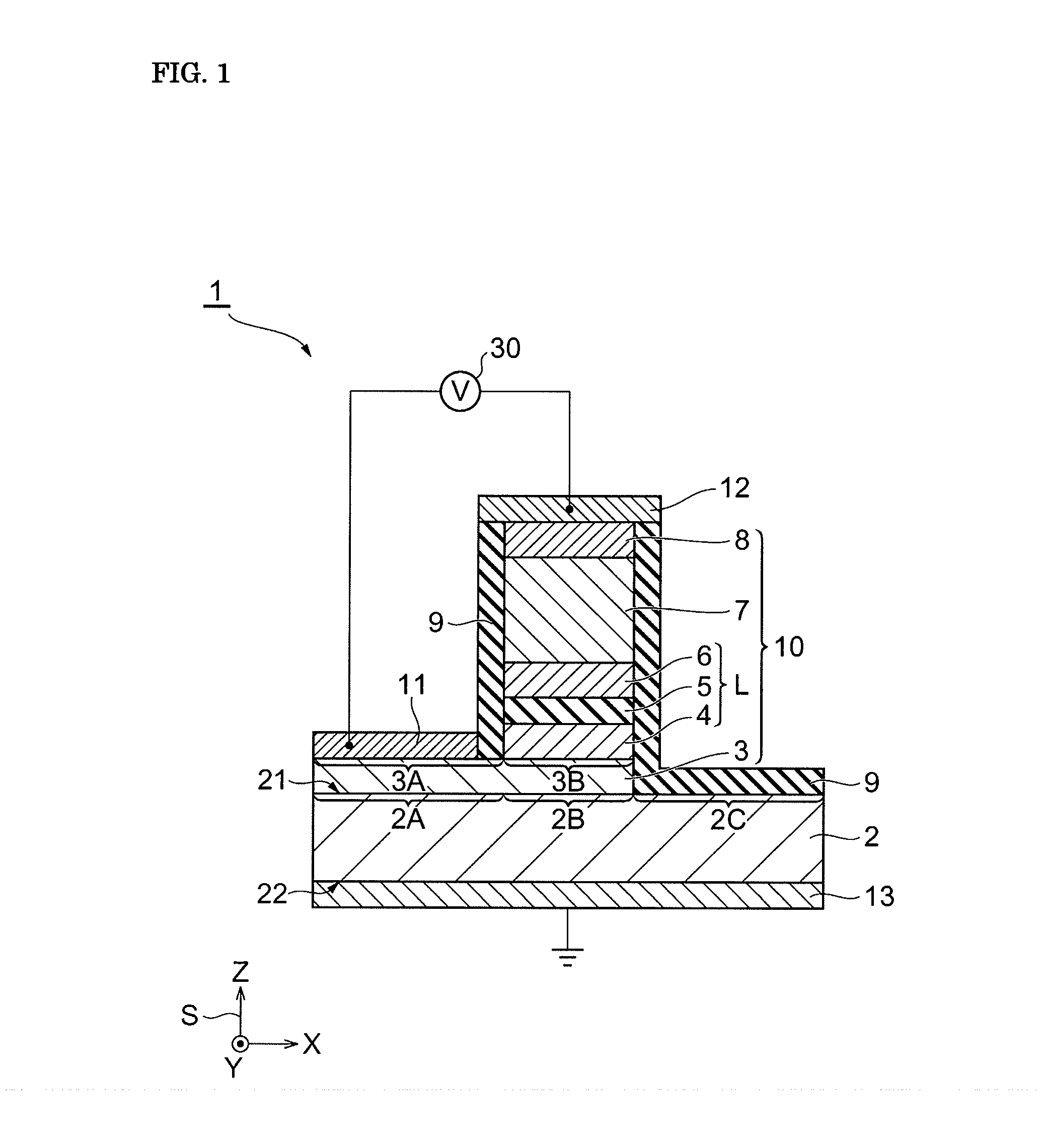
[0007]In the semiconductor optical modulation device according to the above aspect, the optical waveguide layer includes the first semiconductor optical confinement layer, the second semiconductor optical confinement layer, and the insulating layer disposed between the first and second semiconductor optical confinement
layers. The insulating layer is made of aluminum
oxide. Thus, the insulating layer has a larger bandgap energy than the first and second semiconductor cladding
layers and the first and second semiconductor optical confinement
layers. The insulating layer has a higher resistivity than the first and second semiconductor cladding layers and the first and second semiconductor optical confinement layers. This prevents carriers or current from flowing through the insulating layer.
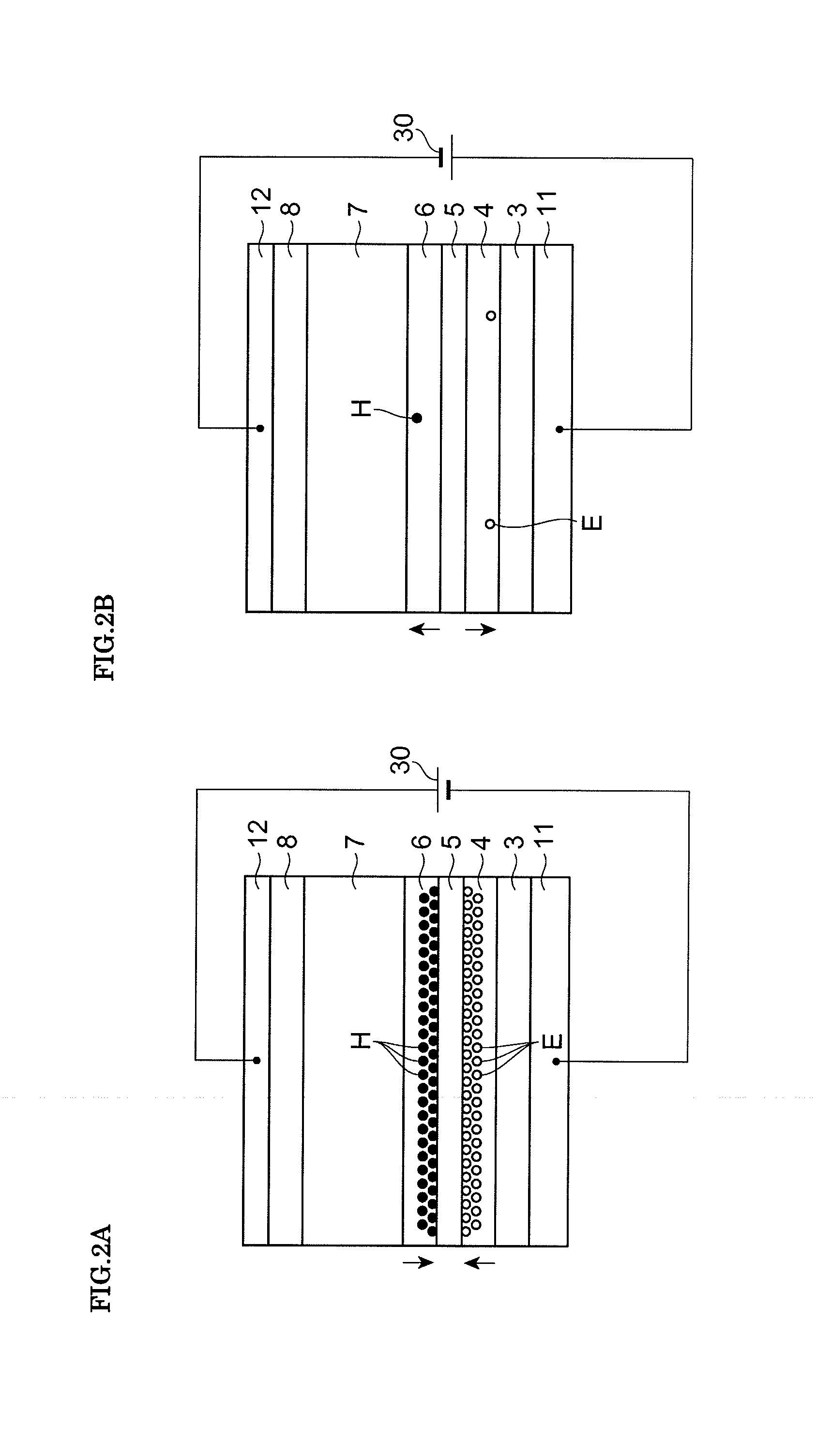
[0008]Assume that the first
conductivity type is n-type and the second conductivity type is p-type. In this semiconductor optical modulation device, if a
negative voltage is applied to the first
electrode and a positive
voltage is applied to the second electrode, carries (in this example, electrons) are injected from the first semiconductor cladding layer (in this example, n-type) to the first semiconductor optical confinement layer. On the other hand, carries (in this example, holes) are injected from the second semiconductor cladding layer (in this example, p-type) to the second semiconductor optical confinement layer. Accordingly, carriers (in this example, electrons) are accumulated in the first semiconductor optical confinement layer, and carriers (in this example, holes) are accumulated in the second semiconductor optical confinement layer. This produces the carrier
plasma effect to decrease the refractive index of the first and second semiconductor optical confinement layers.
[0011]In the semiconductor optical modulation device according to the above aspect, the insulating layer may have a thickness of 5 to 50 nm. In addition, the first semiconductor optical confinement layer and the second semiconductor optical confinement layer may each have a thickness of 20 to 100 nm. In addition, the average refractive index nave of the optical waveguide layer constituted by the first semiconductor optical confinement layer, the insulating layer, and the second semiconductor optical confinement layer may be higher than the refractive indices of the first semiconductor cladding layer and the second semiconductor cladding layer. In the semiconductor optical modulation device according to the above aspect, light propagating in the optical waveguide layer can be effectively confined therein.
[0018]In the Mach-Zehnder interferometer type semiconductor
optical modulator according to the above aspect, preferably, the two optical input ports and two optical output ports of each of the first and second MMI couplers form a through-port and a cross-port with each other, the first and second MMI couplers are configured to
delay the phase of light traveling through the cross-port by 90° and not to shift the phase of light traveling through the through-port, and the first arm has a longer
optical path length than the second arm by the length equivalent to a phase
delay of 90°. According to the above aspect, a Mach-Zehnder interferometer type semiconductor optical modulator capable of on / off operation can be easily provided.
[0020]In the method for producing a semiconductor optical modulation device according to the above aspect, after the semiconductor region including the first semiconductor optical confinement layer, the group III-V
compound semiconductor layer, and the second semiconductor optical confinement layer is formed, the group III-V
compound semiconductor layer in the semiconductor region is oxidized. The group III-V
compound semiconductor layer, which contains aluminum as a group III element, can be easily oxidized. Thus, the insulating layer can be easily formed between the first semiconductor optical confinement layer and the second semiconductor optical confinement layer.

