Semiconductor light emitting device
- Summary
- Abstract
- Description
- Claims
- Application Information
AI Technical Summary
Benefits of technology
Problems solved by technology
Method used
Image
Examples
first embodiment
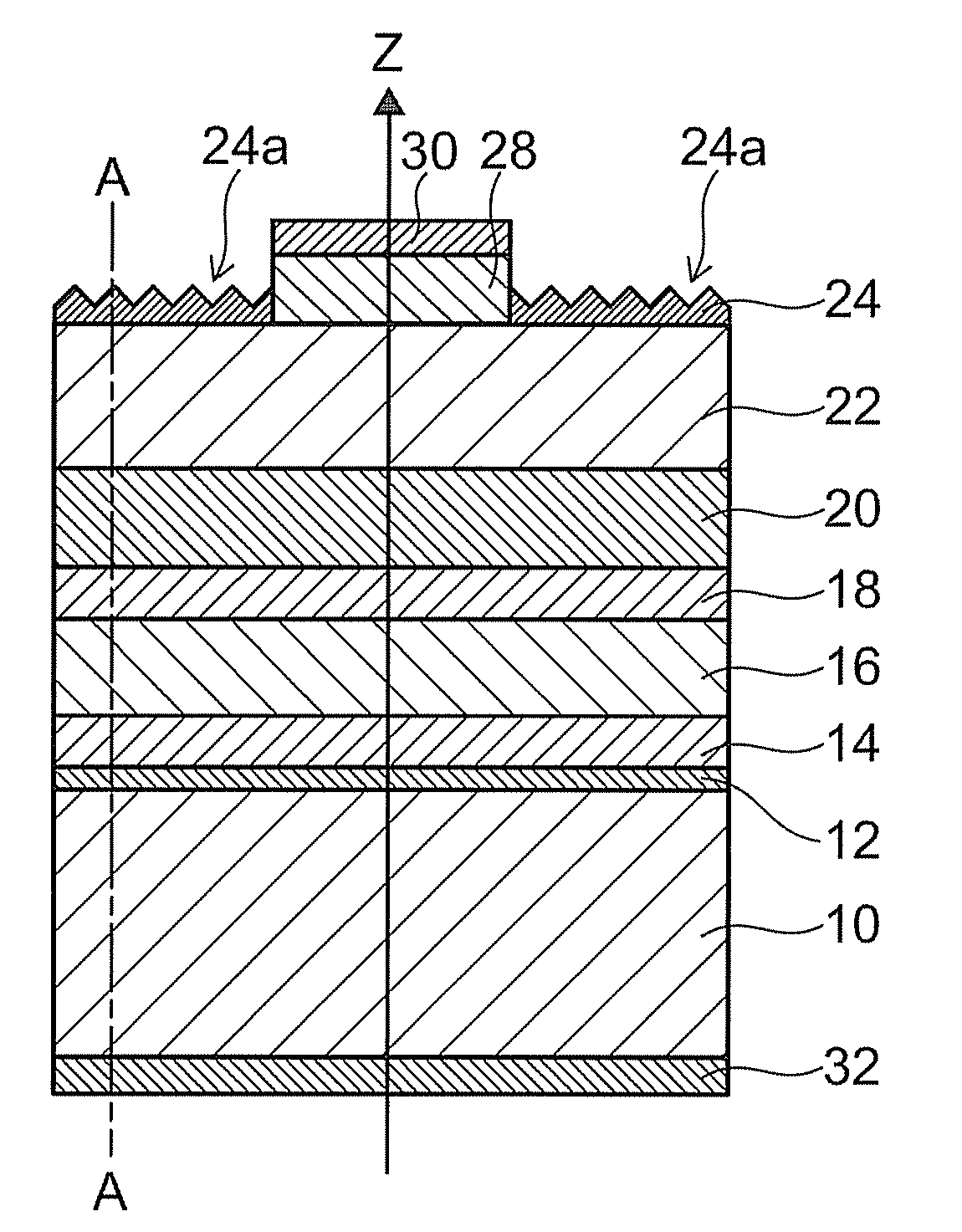
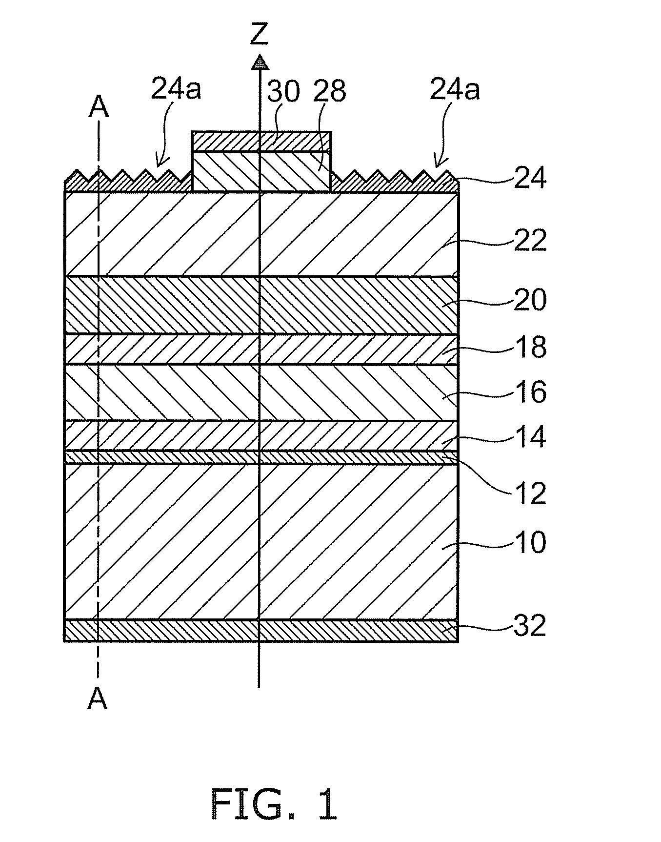
[0023]FIG. 1 is a schematic cross-sectional view of a semiconductor light emitting device according to the invention.
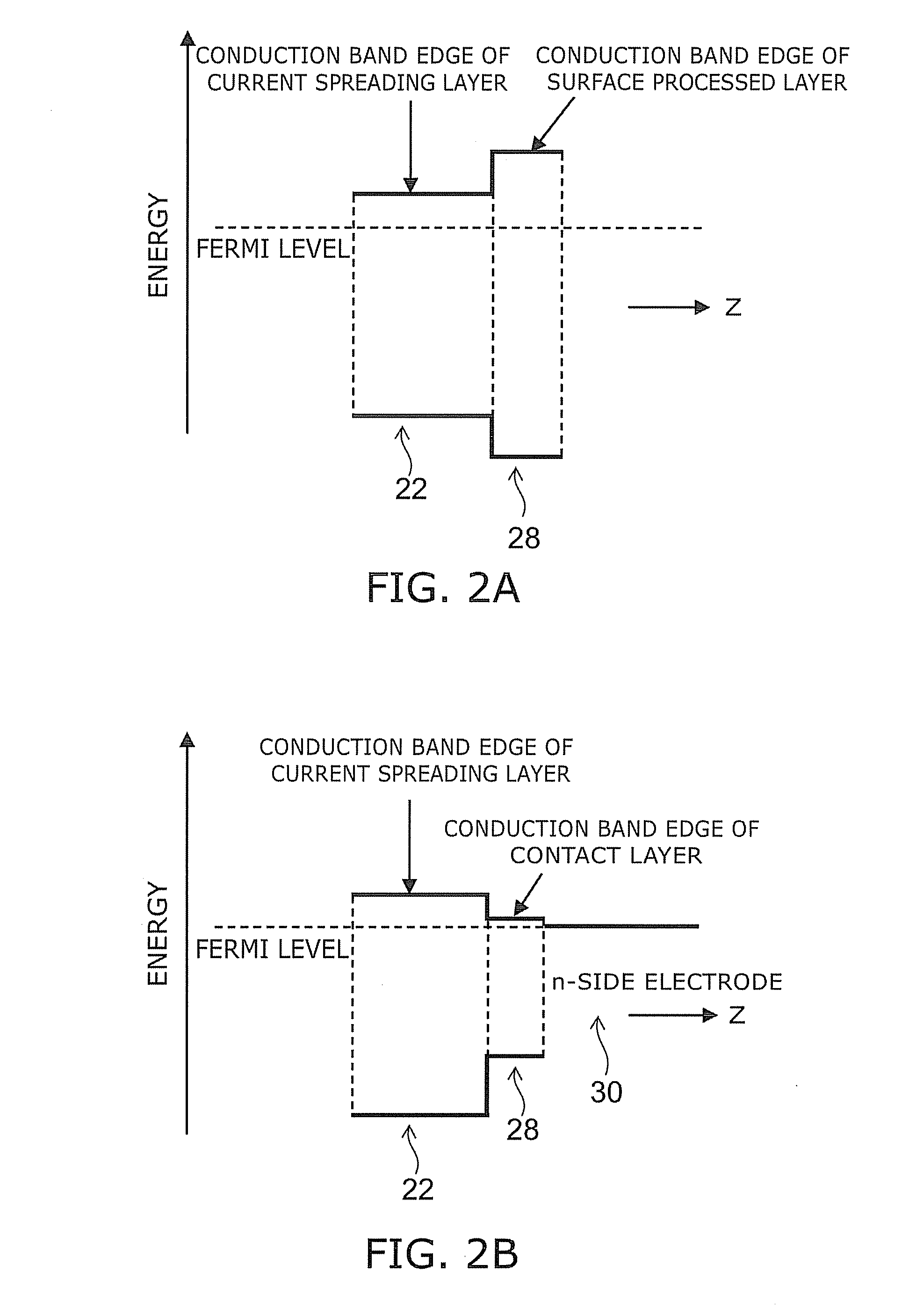
[0024]The semiconductor light emitting device includes a substrate 10 illustratively made of p-type GaAs, on which a heterobarrier-lowering layer 12 of p-type InGaP, a reflecting layer 14 of p-type In0.5Al0.5P / InGaAlP, a cladding layer 16 of p-type In0.5Al0.5P, an active layer 18 made of quantum wells of p-type InGaAlP, a cladding layer 20 of n-type In0.5Al0.5P, a current spreading layer 22 of n-type In0.5(Ga0.7Al0.3)0.5P, and a surface processed layer 24 of n-type In0.5(Ga0.3Al0.7)0.5P formed in this order. Crystal growth technique such as MOCVD (metal organic chemical vapor deposition) or MBE (molecular beam epitaxy) can be used to grow the structure described above.
[0025]If the lattice constant of an InGaAlP-based material is significantly different from that of GaAs, a misfit dislocation is induced into the InGaAlP layer, resulting in deterioration of InGaAlP crys...
second embodiment
[0044]FIG. 5 is a schematic cross-sectional view of a semiconductor light emitting device according to a
[0045]The substrate 10, the heterobarrier-lowering layer 12, the reflecting layer 14, the cladding layer 16, the active layer 18, and the cladding layer 20 have almost the same Al compositions as those of the first embodiment. The current spreading layer 22 is made of n-type Ga0.2Al0.8As, an intermediate layer 23 is made of n-type Ga0.5Al0.5As, and the surface processed layer 24 is made of n-type InGaAlP (x=0.7). A contact layer 28 of GaAs and an n-side electrode 30 are formed on the surface processed layer 24.
[0046]The bandgap of the current spreading layer 22 is larger than that of the active layer corresponding to the emission wavelength (2.0 eV), and its carrier concentration is 1×1018 cm−3. The Al composition x of this current spreading layer 22 is as high as 0.8. Thus, the current spreading layer 22 is easy to oxidize and degradate if it is located near the surface. The inte...
third embodiment
[0052]FIG. 6 is a schematic cross-sectional view of a semiconductor light emitting device according to a
[0053]This embodiment has a structure in which an Au electrode 50, 50b formed on a substrate 52 of Si is bonded to an Au electrode 48, 48b formed on an InGaAlP material. FIG. 6A shows the central region of the device including the n-side electrode 30, and FIG. 6B shows the surrounding region of the central region. The central region of FIG. 6A includes an SiO2 layer 46 adjacent to the Au electrode 48, a current spreading layer 40 of p-type InGaAlP (x=0.3), a cladding layer 16 of p-type In0.5Al0.5P, an active layer 18 made of a p-type InGaAlP quantum well, a cladding layer 20 of n-type In0.5Al0.5P, a current spreading layer 22 of n-type InGaAlP (x=0.3), a surface processed layer 25 of n-type InGaAlP (x=0.7), a contact layer 28 of n-type GaAs, and an n-side electrode 30.
[0054]In the surrounding region of FIG. 6B, the SiO2 layer is removed and replaced by a heterobarrier-lowering lay...
PUM
 Abstract
Description
Claims
Application Information


