
Supplying a clock signal and a gated clock signal to synchronous elements

a clock signal and gated clock technology, applied in the field of data processing, can solve the problems of loss of circuitry state, large power consumption of clock signals, and significant power consumption, and achieve the effect of reducing area and routing overheads

Active Publication Date: 2013-03-05
ARM LTD
View PDF20 Cites 8 Cited by
  • Summary
  • Abstract
  • Description
  • Claims
  • Application Information

AI Technical Summary

Benefits of technology

The present invention provides a clock gating circuit that can be used to send a gated clock signal to certain elements in response to a low power mode signal. By doing so, the circuit can provide secure state retention for these elements when surrounding elements are powered down. This helps to reduce power consumption and routing overheads. The circuit can also be easily integrated into standard cell libraries, making it suitable for various integrated circuits. The invention provides a solution for reducing power consumption and leakage during low power mode while maintaining the necessary state retention for certain elements.

Problems solved by technology

The clock signal consumes a lot of power in a circuit and thus, being able to gate it in certain parts of the circuit that do not require it can save a significant amount of power.
Although this results in substantial power savings it also results in a loss of state within the circuitry.
A disadvantage of this approach is that the balloon latches consume considerable additional circuit area.
This requires a control signal to be sent to each transmission gate and has significant routing overheads.

Method used


Image

  • Supplying a clock signal and a gated clock signal to synchronous elements
  • Supplying a clock signal and a gated clock signal to synchronous elements
  • Supplying a clock signal and a gated clock signal to synchronous elements

Examples


Embodiment Construction

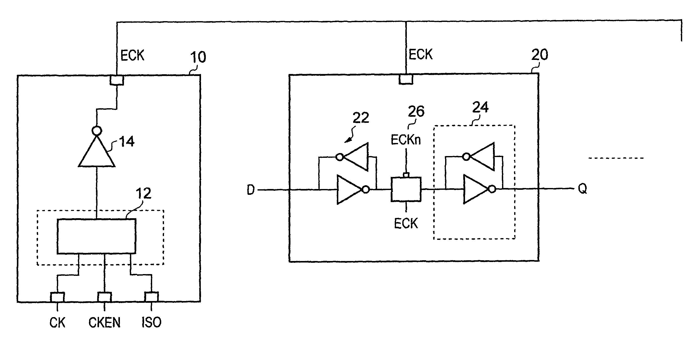
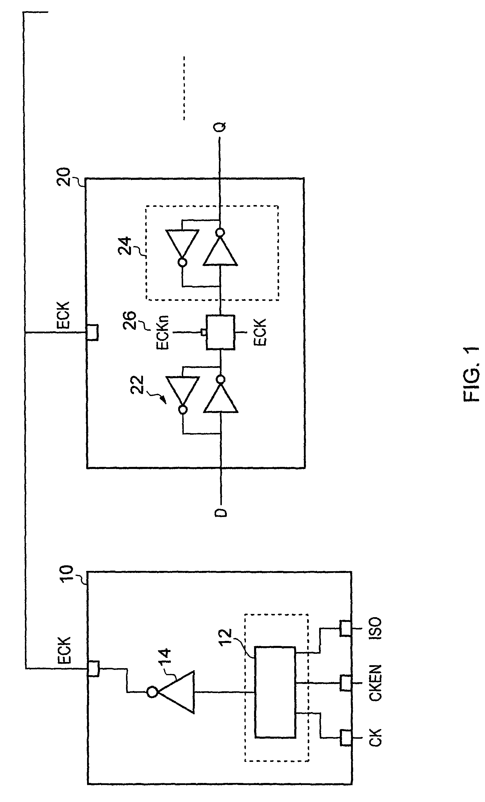
[0055]FIG. 1 shows a clock gating cell 10 supplying a clock signal ECK to a state retention circuit 20. In this embodiment state retention circuit 20 is a master slave flip-flop having a master latch 22 and a slave latch 24. These are separated from each other by transmission gate 26 which receives the clock signal ECK and transmits a data signal from the master latch 22 to the slave match 24 in response to the clock signal ECK being high and isolates the slave latch 24 from the master latch 22 in response to the clock signal ECK being low. In this figure elements surrounded by the non-continuous line are powered by a first power supply that is constantly powered while those not surrounded by the non-continuous line are powered by a second power supply that is powered down in a low power standby mode.

[0056]Clock gating cell 10 is formed of logic circuitry 12 which receives a clock signal CK a clock enable signal CKEN and a low power isolation signal ISO. It also has an inverter 14. ...


PUM


Abstract

A clock gating circuitry is configured to receive a clock signal and to output an output signal comprising either the clock signal or the predetermined gated value. The circuitry receives a clock signal, a clock enable signal having either an enable value or a disable value, and a power mode signal having either a low power value (indicating entry to a low power mode in which at least a portion of the plurality of synchronous elements are powered to retain data and are not clocked and at least a further portion of the plurality of synchronous elements are powered down), or a functional mode value (indicating the plurality of synchronous elements are to be powered). A clock gating unit has logic circuitry that is configured to output the clock signal or the predetermined gated value depending upon the low power value and the functional mode value.

Description

BACKGROUND OF THE INVENTION[0001]1. Field of the Invention[0002]The field of the invention relates to the field of data processing and in particular, to reducing power consumption in data processing circuitry by gating the clock signal supplied to portions of the circuitry when they are not active.[0003]2. Description of the Prior Art[0004]In many circuits, particularly those that run off remote power supplies such as batteries, it is important to keep the power consumption of the circuits low. One way of doing this has been to gate the clock signal supplied to synchronous elements when they are not operational. The clock signal consumes a lot of power in a circuit and thus, being able to gate it in certain parts of the circuit that do not require it can save a significant amount of power.[0005]In modem circuits a clock signal is often supplied to several synchronous elements via a clock gating cell. These cells are controlled by their own clock enable signal and in response to this...

Claims


Application Information

Patent Timeline
Patent Type & Authority Patents(United States)
IPC IPC(8): H03K19/00
CPCG06F17/5059H03K19/0013H03K19/0016G06F2217/62G06F2217/78G06F2217/84G06F30/35G06F30/396G06F2119/12G06F2119/06G06F1/32H03K3/037
Inventor MYERS, JAMES EDWARDFLYNN, DAVID WALTERAITKEN, ROBERT CAMPBELLFREDERICK, JR., MARLIN WAYNE
Owner ARM LTD
Learn More