Method and apparatus of operating a non-volatile DRAM

a non-volatile and memory technology, applied in static storage, digital storage, instruments, etc., can solve the problems of inability to retain data without periodic refresh process, complicated system design, etc., and achieve fast random access of volatile memory cells and fast read and write access

Active Publication Date: 2013-03-05
CHIP MEMORY TECH
View PDF29 Cites 18 Cited by
  • Summary
  • Abstract
  • Description
  • Claims
  • Application Information

AI Technical Summary

Benefits of technology

[0020]An object of this invention is to provide a non-volatile DRAM cell which provides fast random access of a volatile memory cell and the capability of retaining data of a non-volatile memory. The cell is capable of going through program or erase without affecting the voltage on the common-plate of the cell capacitor or exceeding the maximum voltage across the cell capacitor in the DRAM mode. Preserving the maximum compliance voltage of the capacitor allows the cell to be fabricated using a DRAM process with changes limited to the gate structure of the pass-gate transistor. Another object is to provide a non-volatile DRAM device that consists of multiple rows and columns of the non-volatile DRAM cells such that the memory device can provide fast read and write access similar to that of a DRAM device but can retain data like a non-volatile memory device. Yet another object is to provide a sensing scheme so that the same sense amplifier can be used for both DRAM and NVM read operation. Another objective is to provide a method and apparatus on the non-volatile DRAM device so that, during a program or erase operation, the cell capacitor common-plate voltages is not changed; the data stored in the capacitor of the memory cells in the non-selected row is preserved, and the maximum voltage across the cell capacitors is substantially the same as that when the device is operating in the DRAM mode. The advantage of preserving data stored in the cells capacitors of non-selected rows minimizes the page size of the non-volatile memory program / erase operation to one memory row rather than the whole array as in other prior art schemes such as those described in U.S. Pat. No. 7,099,181 (Ahn, et al.) and U.S. Pat. No. 5,181,188 (Yamauchi et al). Since the memory is capable of row erase and program, the read and write endurance of the memory as a whole, is better than those with array erase / program operation by a factor equal to the array size divided by row size, This is because, when a memory array is accessed, the chance that a bit in a memory block that needs to go through an erase / program cycle is row size / block size in the present embodiment.
[0025]In the memory array, all the cells in a row have their control gates connected to a word line. The cell array is arranged in a folded bit-line structure such that a complementary bit line pair is associated with a column of cells with half of the cells in the column connected to one bit line and the other half connected to the other bit line. The folded bit line arrangement is commonly used in the memory arrays of a DRAM device and is well documented in the DRAM art. In the present embodiment, the memory array incorporates at least one dummy row of non-volatile DRAM cells with their floating gate preconditioned in the program state. The dummy row facilitates non-volatile memory read operations during which data stored in the floating gate of the non-volatile DRAM cells is accessed.
[0026]The non-volatile DRAM device includes a plurality of sense amplifiers for data sensing operations when data is read from the capacitor or the floating gate of the non-volatile DRAM cell. Data sensing in a normal DRAM and a Nonvolatile memory (NVM) is inherently different. Data sensing in a DRAM usually employs charge sensing because the data stored in a DRAM cell is represented by the amount of charge stored in the capacitor of the cell. However, data sensing in a NVM usually employs current sensing because data state represented by the amount of charge trapped in the floating gate is automatically converted into current conducted by the pass-gate transistor when the pass-gate is turned on. Due to the difference between charge and current, data sensing in a DRAM and nonvolatile memory is traditionally different. To reduce the semiconductor circuit area occupied by the sense amplifiers and simply the sensing control logic, it is desirable to use the same sense amplifiers for both DRAM and NVM read operations. In the present embodiment a sensing scheme that can perform sensing operation for data stored in both the floating gate and the capacitor of the cell using the same sense amplifier is provided.

Problems solved by technology

A DRAM has faster random access speed than a non-volatile memory; however, it cannot retain data without a periodic refresh process.
Because the non-volatile and volatile memory have these different characteristics, interface and control of non-volatile and volatile are substantially different and resulting in more complicated system design.

Method used


Image

  • Method and apparatus of operating a non-volatile DRAM
  • Method and apparatus of operating a non-volatile DRAM
  • Method and apparatus of operating a non-volatile DRAM

Examples


Embodiment Construction

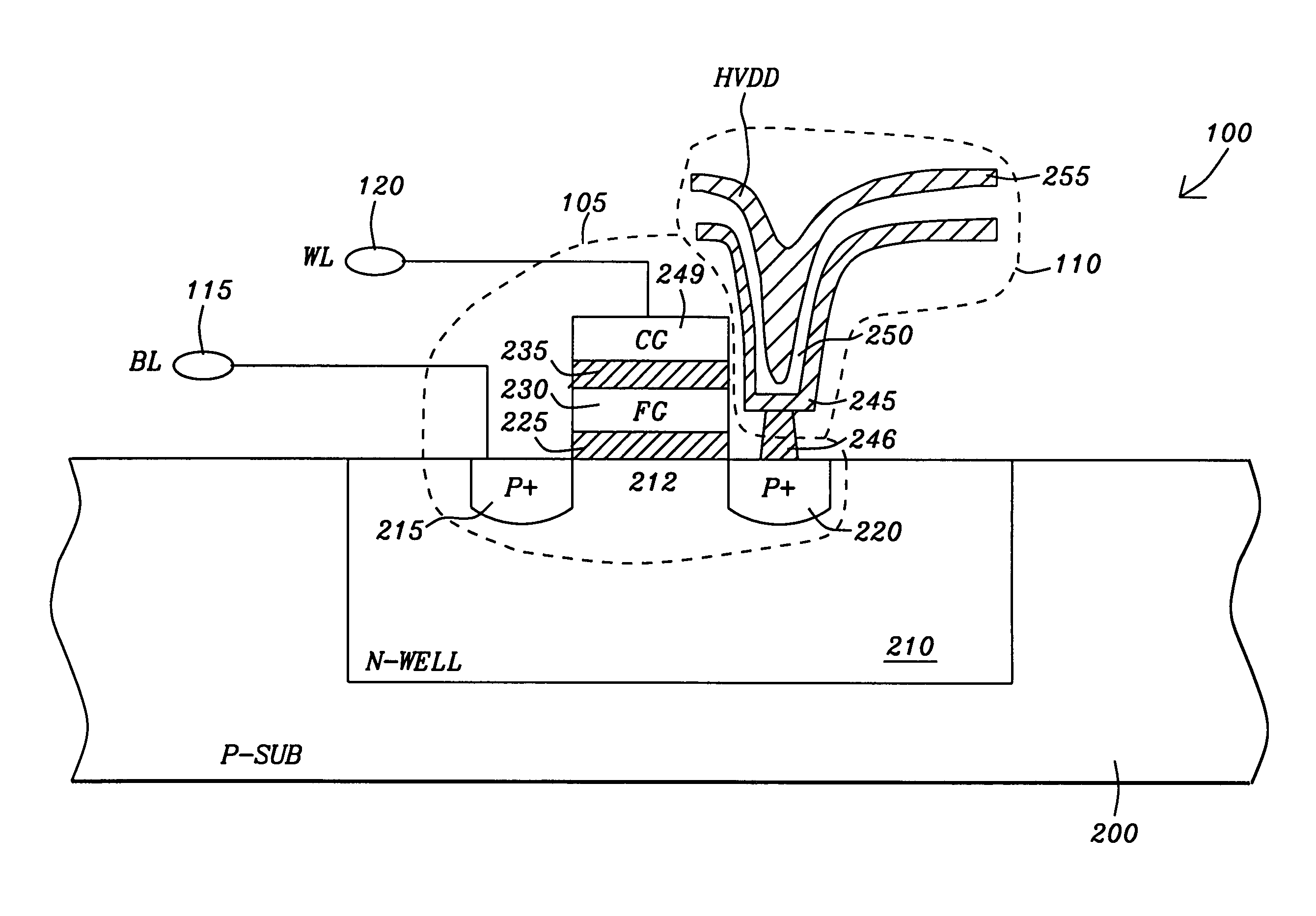
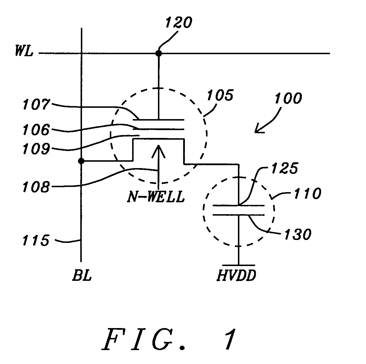
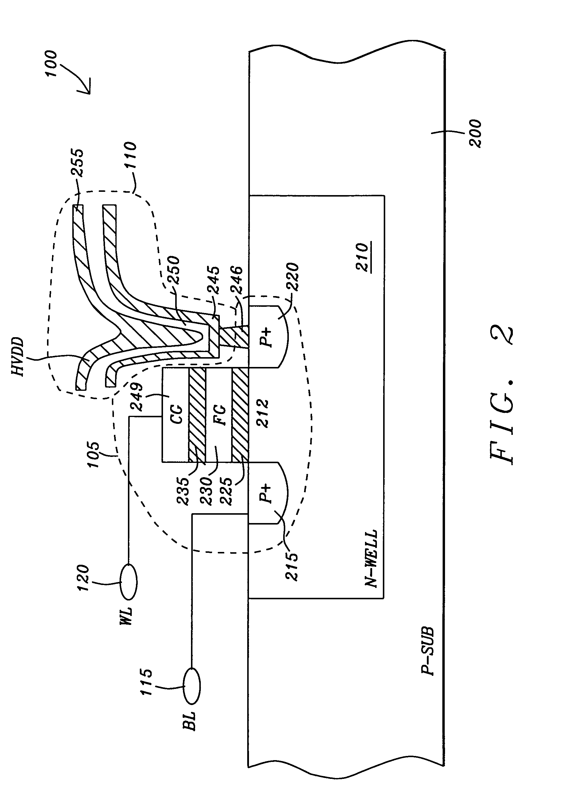
[0041]FIG. 1 shows the schematic of a non-volatile DRAM cell 100 in the present embodiment. It includes a pass-gate transistor 105 and a cell capacitor 110 to provide fast read or write access in the DRAM operating mode and in the NVM operating mode. The non-volatile DRAM cell 100 is arranged similar to a DRAM cell with the drain of the pass-gate transistor 105 connecting to a bit line 115, the source connecting to the bottom plate 125 of the cell capacitor 110 and the control gate connecting to a word line 120. The top capacitor plate 130 is connected to a common-plate node coupled to a voltage source HVDD with a voltage approximately equal to one half of the voltage level of the power supply voltage (VDD / 2). The pass-gate transistor 105 functions as the selection transistor and the cell capacitor 110 provides temporary charge storage when the non-volatile DRAM cell 100 is operating in the DRAM mode. The pass-gate transistor 105 contains a floating gate 106 and a control gate 107. ...


PUM


Abstract

A non-volatile DRAM cell includes a pass-gate transistor and a cell capacitor. A read operation of the non-volatile cell begins by positively charging the cell capacitor. A cell capacitor of an associated dummy non-volatile DRAM cell is fully charged. The pass-gate transistor is activated and if the pass-gate transistor is erased it does not turn on and if it is programmed, it turns on. Charge is shared on the complementary pair of pre-charged bit lines connected to the non-volatile DRAM cell and its associated Dummy non-volatile DRAM cell. A sense amplifier detects the difference in the data state stored in the pass-gate transistor. The program and erase of the non-volatile DRAM cell is accomplished Gate-induced drain-lowering (GIDL) assisted band-to-band tunneling and Fowler-Nordheim tunneling respectively. Programming or erasing a selected row of cells does not affect the data states of the cells in the unselected rows.

Description

[0001]This application claims priority under 35 U.S.C. §120 and 37 CFR §1.78 as a continuation-in-part to U.S. patent application Ser. No. 12 / 316,436, filed Dec. 12, 2008, now U.S. Pat. No. 8,059,471 which in turn claims priority under 35 U.S.C. §119 to U.S. Provisional Patent Application Ser. No. 61 / 065,446, filed on Feb. 12, 2008, both of which are herein incorporated by reference in their entirety.BACKGROUND OF THE INVENTION[0002]1. Field of the Invention[0003]This invention relates generally to non-volatile dynamic random access memories (DRAM). More particularly, this invention relates to methods and circuits for operating non-volatile DRAM's.[0004]2. Description of Related Art[0005]The alternative to the non-volatile memories are volatile memories such as Static Random Access Memory (SRAM) and Dynamic Random Access Memory (DRAM). The volatile memories generally have a greater accessing speed. A DRAM has faster random access speed than a non-volatile memory; however, it cannot ...

Claims


Application Information

Patent Timeline
Patent Type & Authority Patents(United States)
IPC IPC(8): G11C11/34G11C16/04
CPCG11C11/404G11C11/4072G11C11/4076G11C14/0018G11C16/0416G11C16/10
Inventor LEUNG, WINGYU
Owner CHIP MEMORY TECH
Why Eureka
Try Eureka