Buffer and display device

a display device and buffer technology, applied in the field of buffers, can solve the problems of increased consumption current and delay in output output output output, and achieve the effect of increasing the resistance of a current path

Active Publication Date: 2013-04-23
SHARP KK
View PDF13 Cites 9 Cited by
  • Summary
  • Abstract
  • Description
  • Claims
  • Application Information

AI Technical Summary

Benefits of technology

[0020]In order to reduce such delay in the outputting, it is required that a current drive for the buffer be enhanced by replacing the resistor having the high resistance value with a resistor having a lower resistance value or a transistor having a large channel width W. However, after all, this will remove the counter-measures employed against the pass-through current, thereby resulting in an increase in the consumption current.
[0076]The invention brings about an effect that realizes the display device including the level shifter circuit in which it is possible that the consumption current be reduced and the load be sufficiently driven.

Problems solved by technology

In a case where the output terminal OUT is connected to a large capacitive load, this causes a delay in outputting from the output terminal OUT.
In order to reduce such delay in the outputting, it is required that a current drive for the buffer be enhanced by replacing the resistor having the high resistance value with a resistor having a lower resistance value or a transistor having a large channel width W. However, after all, this will remove the counter-measures employed against the pass-through current, thereby resulting in an increase in the consumption current.

Method used


Image

  • Buffer and display device
  • Buffer and display device
  • Buffer and display device

Examples


Embodiment Construction

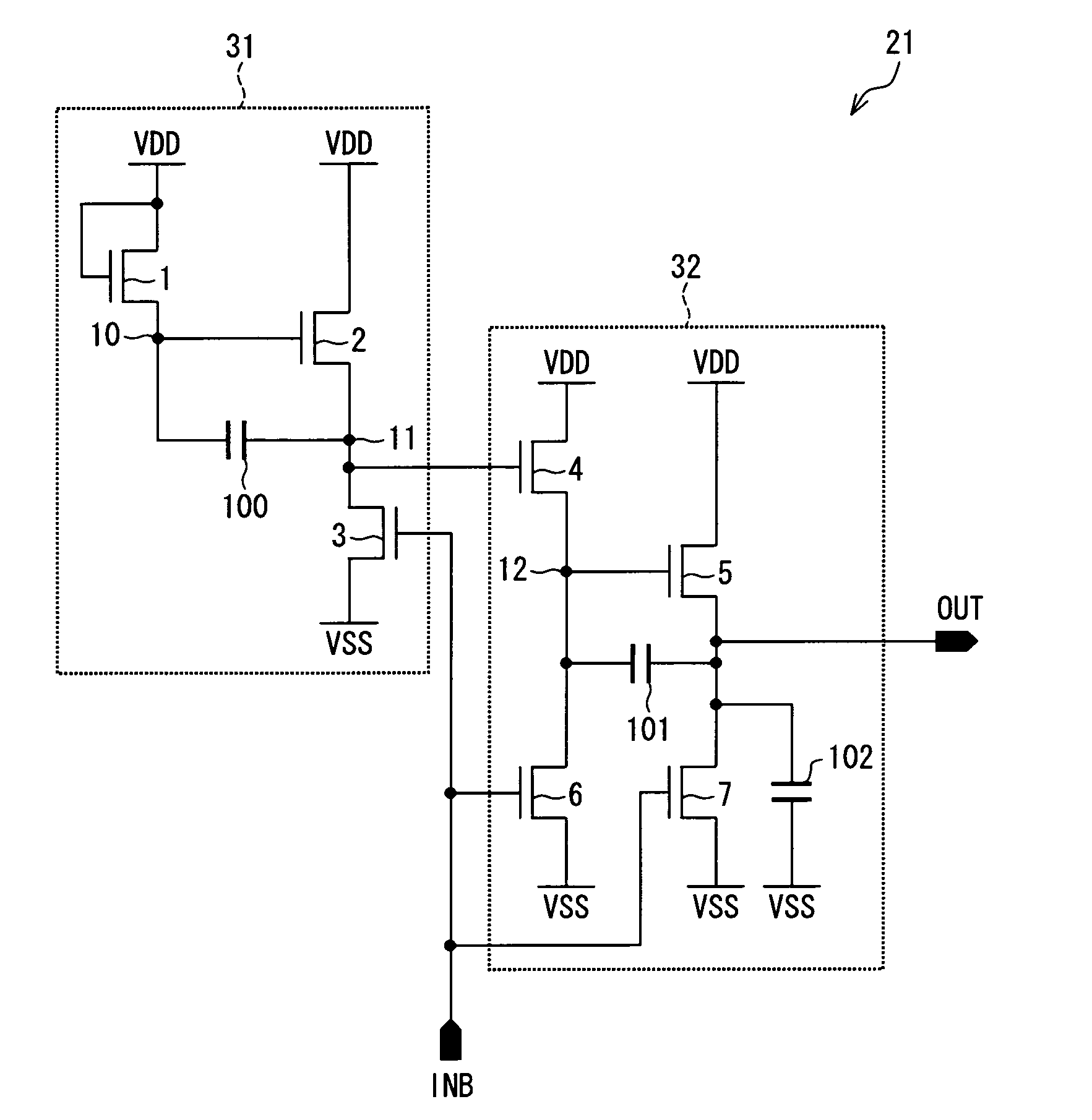
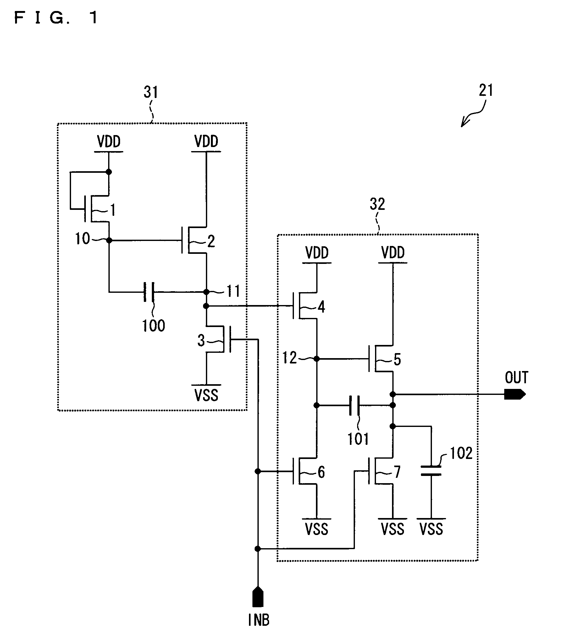
[0121]One embodiment of the present invention is described as follows, with references to FIGS. 1 through 17 and 23 through 30.

[0122]FIG. 17 shows a configuration of a liquid crystal display device (display device) 151 in accordance with the present embodiment.

[0123]The liquid crystal display device 151 includes a panel 152 on which a pixel region 153 is formed, and includes, on the panel 152, a source driver 154, a gate driver 155, a BUFF / level shifter circuit 156, a power supply circuit 157, and terminals 158. The source driver 154 includes an output circuit 154a for outputting data signals for respective source bus lines of the pixel region 153. The gate driver 155 includes an output circuit 155a for outputting selection signals to respective gate bus lines so that the data signals from the source driver 154 are written down into corresponding pixels of the pixel region 153. The output circuits 154a and 155a are each formed by a buffer having a low output impedance, which serves ...


PUM


Abstract

A single-phase input including transistors all of which have only a single type of channel polarity, which buffer includes: a buffer section 32, including a first series circuit formed by two n-channel transistors connected to each other in series, a second series circuit formed by two n-channel transistors connected to each other in series at a connection point OUT, and a capacitor; and an inverted-signal generating section for generating an inverted-signal from an input signal, the inverted-signal generating section including n-channel transistors but no p-channel transistor, the input signal being inputted to respective gates of the transistors, the inverted-signal being inputted to a gate of the transistor 4, and an output signal being outputted via the connection point OUT. With the buffer, it is possible that a consumption current be reduced and a current drive for a load is enhanced.

Description

TECHNICAL FIELD[0001]The present invention relates to a buffer including transistors all of which have only a single type of channel polarity.BACKGROUND ART[0002]A liquid crystal display device may include a buffer having a low output impedance and outputting an amplified (in broad sense of the term) signal. A member so called buffer can be a level-shifter for performing a translation of a source voltage or an amplifier for receiving an input signal and outputting an amplified signal with unity gain. In a case where the buffer includes CMOS transistors, it is required that p-channel transistors and n-channel transistors be formed in respective processes. The buffer may include transistors all of which have only a single type of channel polarity, such as n-channel, so that the forming steps can be simplified (see, for example, Patent Literature 1).[0003]FIGS. 18 and 19 each show an example of a configuration of a buffer which includes n-channel transistors but no p-channel transistor...

Claims


Application Information

Patent Timeline
Patent Type & Authority Patents(United States)
IPC IPC(8): H03K3/00
CPCG09G3/3677H03K19/09441H03K19/01714H03K19/018507H03K19/0013G09G2310/0291G09G2330/021
Inventor YAMAMOTO, ETSUOMURAKAMI, YUHICHIROHSASAKI, YASUSHIGYOUTEN, SEIJIROUSHIMIZU, SHINSAKU
Owner SHARP KK
Why Eureka
Try Eureka