ESD networks for solder bump integrated circuits

a technology of integrated circuits and solder bumps, applied in the field of integrated circuits and semiconductor dice, can solve the problems of long interconnect lengths and complex routing that can take up die area, and achieve the effect of reducing the average interconnect length

Active Publication Date: 2013-04-23
NXP BV
View PDF10 Cites 4 Cited by
  • Summary
  • Abstract
  • Description
  • Claims
  • Application Information

AI Technical Summary

Benefits of technology

[0005]Various aspects of the present invention are directed to integrated circuit chips that include semiconductor dice having an interior area bounded by a peripheral area, such semiconductor dice including at least one functional domain located in the die interior area and I / O circuitry providing I / O interconnects for the at least one functional domain. In accordance with various aspects of the present invention, the I / O circuitry includes a plurality of solder bump pads without including peripheral wire bond pads, and at least a portion of the bump pads are interior bump pads distributed over the die interior area. An ESD network is provided to protect components of the die from electrostatic discharge, the ESD network including a plurality of ESD structures located in the die interior area, each of the ESD structures placed proximate to respective power and ground connections, and positioned to reduce an average interconnect length between the interior bump pads and the ESD structures relative to an average path length between the interior bump pads and the die peripheral area.
[0006]Various aspects of the present invention are further directed to methods for designing integrated circuit chips including a semiconductor die having an interior area bounded by a peripheral area and at least one functional domain located in the die interior area. Such methods include distributing solder bump pads over a surface of the die to provide the I / O interconnects for the at least one functional domain without including peripheral wire bond pads, at least a portion of the bump pads being interior bump pads distributed over the die interior area. Such methods further includes providing an ESD network of ESD structures to protect components of the die from electrostatic discharge, at least a portion of the ESD structures located in the die interior area, each of the ESD structures being placed proximate to respective power and ground connections and being positioned to reduce an average interconnect length between the interior bump pads and the ESD structures relative to an average path length between the interior bump pads and the die peripheral area.

Problems solved by technology

When such semiconductor dice are also provided with bump pads for use in flip-chip configuration, bump pads distributed over the interior area are routed to the ESD ring, resulting in long interconnect lengths and often complex routing that can take up die area.

Method used


Image

  • ESD networks for solder bump integrated circuits
  • ESD networks for solder bump integrated circuits
  • ESD networks for solder bump integrated circuits

Examples


Embodiment Construction

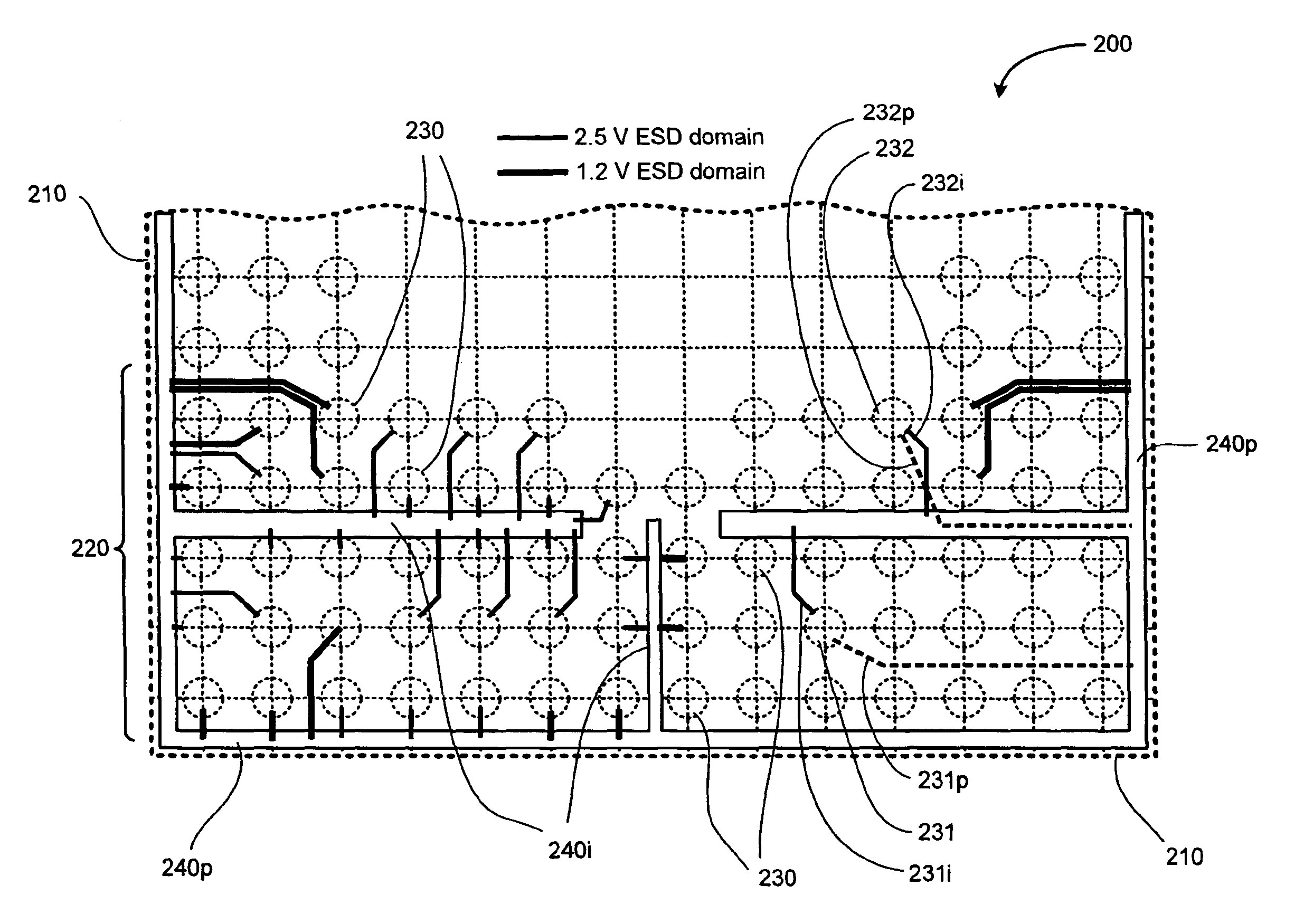
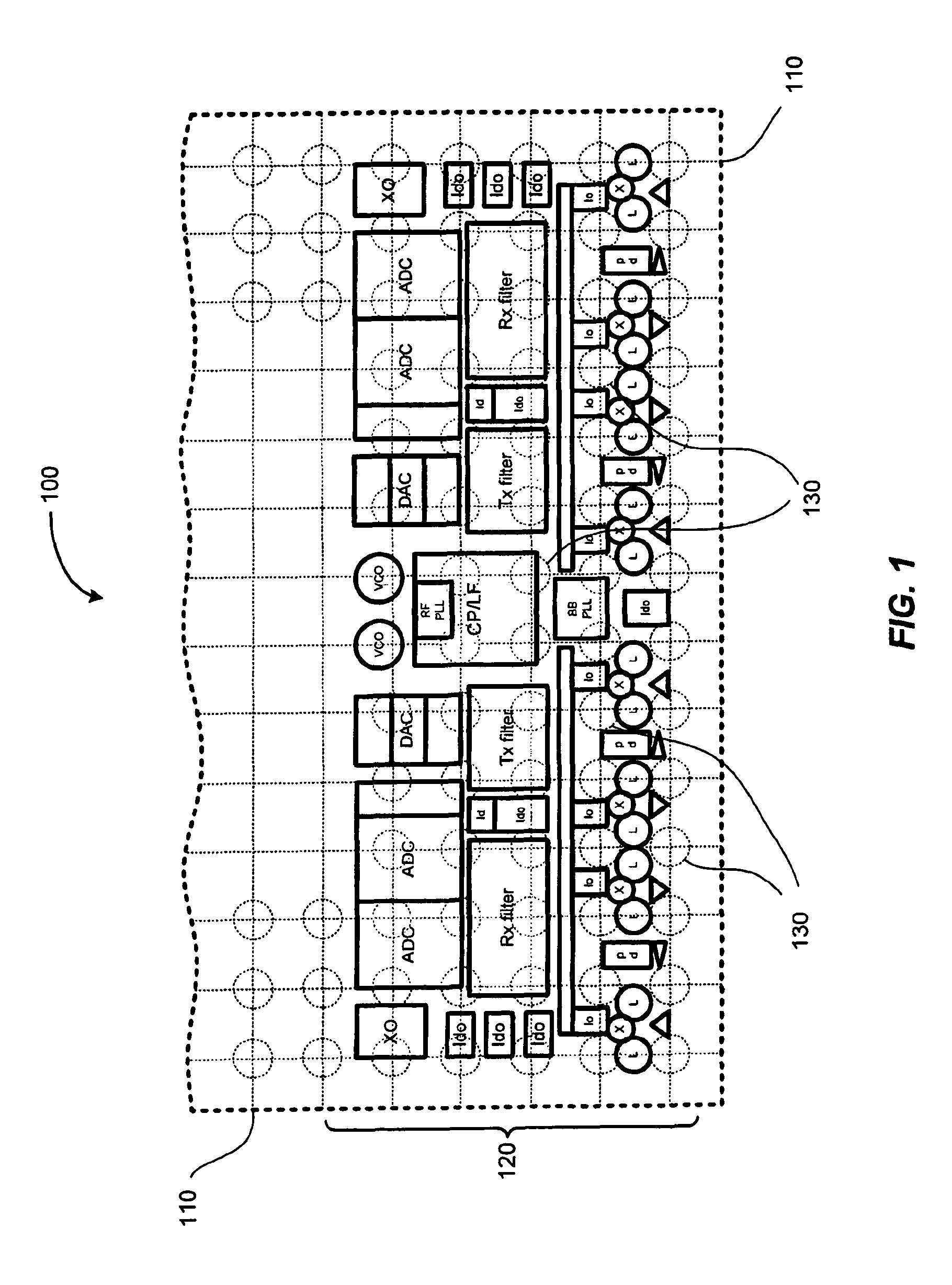
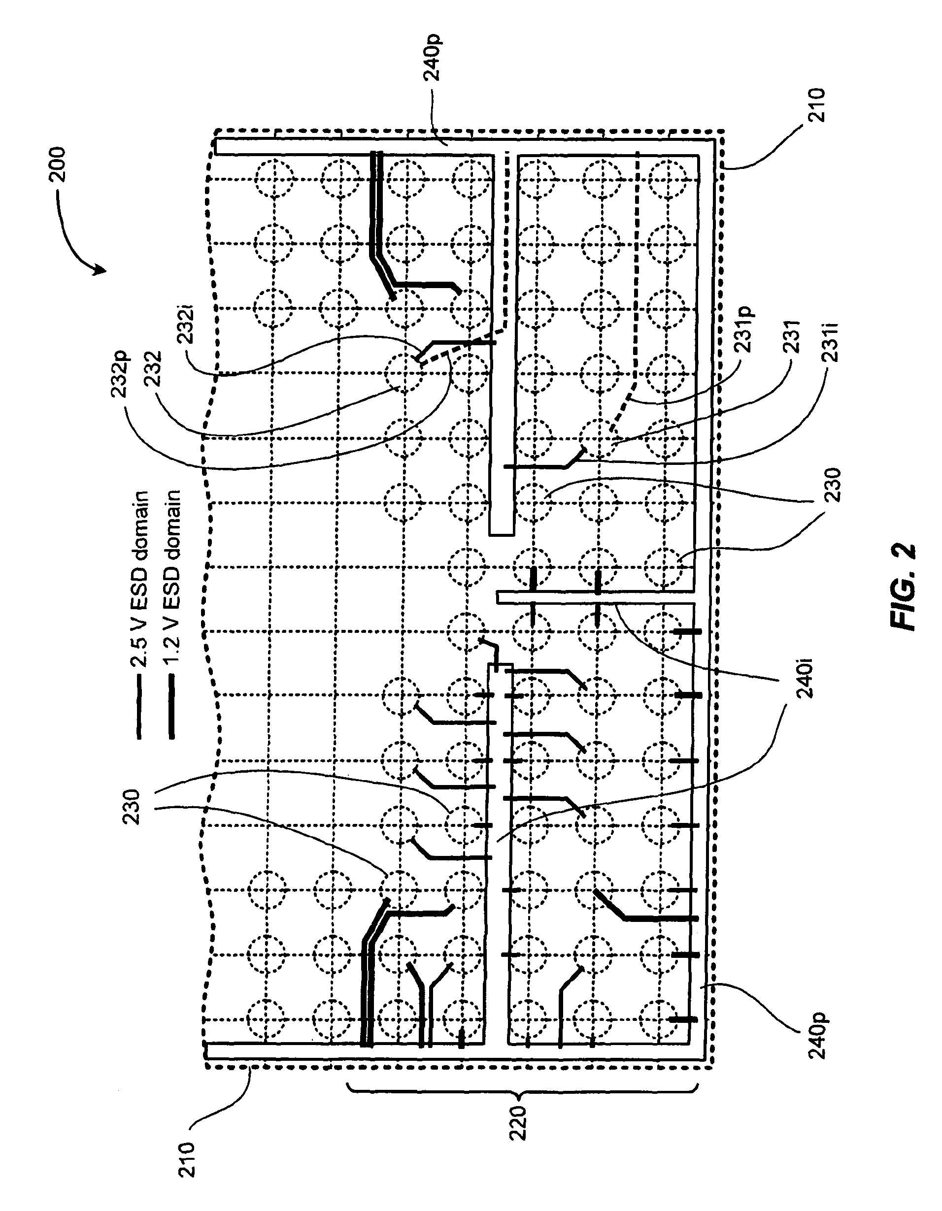
[0012]Embodiments of the present invention relate to integrated circuits and semiconductor dice that include at least one functional domain in the die interior area and I / O circuitry providing I / O interconnects for the at least one functional domain, the I / O circuitry including a plurality of solder bump pads without including peripheral wire bond pads, at least a portion of the bump pads being interior bump pads distributed over the die interior area. In accordance with certain embodiments, ICs and dice of the present invention further include an ESD network to protect components of the die from electrostatic discharge, the ESD network including a plurality of ESD structures located in the die interior area, each of the ESD structures placed proximate to respective power and ground connections and positioned to reduce an average interconnect length between the interior bump pads and the ESD structures relative to an average path length between the interior bump pads and the die per...


PUM


Abstract

Semiconductor dice (100, 200) of integrated circuit chips are provided with solder bump pads (130, 230) distributed over active areas of the dice to supply the I / O interconnects without including peripheral wire bond pads. The dice are further provided with protective ESD structures (140p / 140i, 240p / 240i) arranged in a network that includes ESD structures that extend into the interior areas of the dice. This allows the ESD structures to be placed proximate to respective power and ground connections, and positioned to reduce an average interconnect length between interior bump pads and the ESD structures relative to an average path length between the interior bump pads and the die peripheral area.

Description

FIELD OF THE INVENTION[0001]The present invention relates generally to integrated circuits and semiconductor dice that include protective ESD structures and solder bumps for external interconnecting.BACKGROUND OF THE INVENTION[0002]In conventional integrated circuit technology, interconnections are made using wire bond pads arranged in one or more rows around the periphery of the semiconductor die, or using solder bump pads arranged in an array over the circuit area of the die. The trend in the electronics industry is to increase reliance on solder bump connections. Often, existing circuit designs that originally utilized wire bonding are retrofitted for solder bumps or are made with the solder bumps as an option in addition to the conventional wire bonding assembly.[0003]Together with the provided wire bond pads, there is circuitry that protects the interior parts of the circuit from electrostatic discharge (ESD) events, for example that can occur during handling of the circuit die...

Claims


Application Information

Patent Timeline
Patent Type & Authority Patents(United States)
IPC IPC(8): H02H9/00H02H1/00H02H1/04H02H3/22H02H9/06
CPCH01L23/585H01L23/60H01L27/0251H01L2924/0002H01L2924/00
Inventor CHARLON, OLIVER
Owner NXP BV
Why Eureka
Try Eureka