Three dimensional CMOS integrated circuits having device layers built on different crystal oriented wafers

A three-dimensional integration and device technology, used in circuits, semiconductor devices, electrical solid devices, etc., can solve problems such as poor electrical properties, difficult to control the surface orientation of the recrystallized layer, and low-level device and circuit performance.

Inactive Publication Date: 2007-10-10
GLOBALFOUNDRIES INC
View PDF6 Cites 0 Cited by
  • Summary
  • Abstract
  • Description
  • Claims
  • Application Information

AI Technical Summary

Problems solved by technology

Circuits fabricated in this way suffer from two major disadvantages: (1) the recrystallized top layer often has poor electrical properties, which may lead to lower device and circuit performance; it is also difficult to control the surface orientation of the recrystallized layer; (2) Thermal cycling from top layer formation to subsequent device fabrication degrades underlying device performance

Method used


Image

  • Three dimensional CMOS integrated circuits having device layers built on different crystal oriented wafers
  • Three dimensional CMOS integrated circuits having device layers built on different crystal oriented wafers
  • Three dimensional CMOS integrated circuits having device layers built on different crystal oriented wafers

Examples


Embodiment Construction

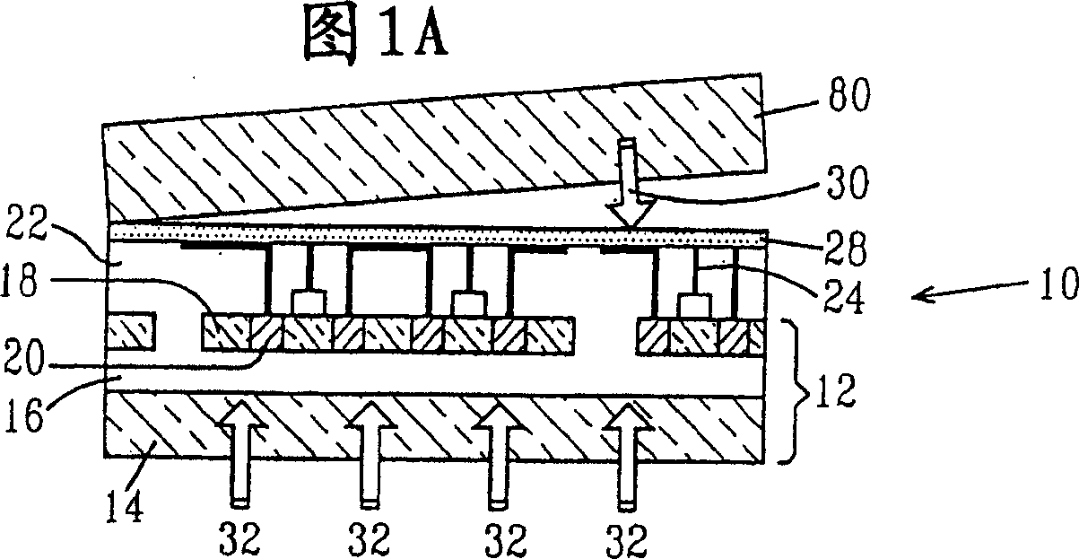
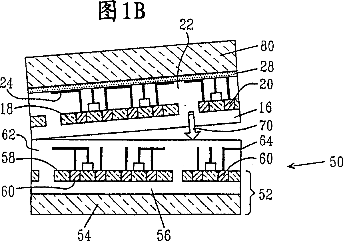
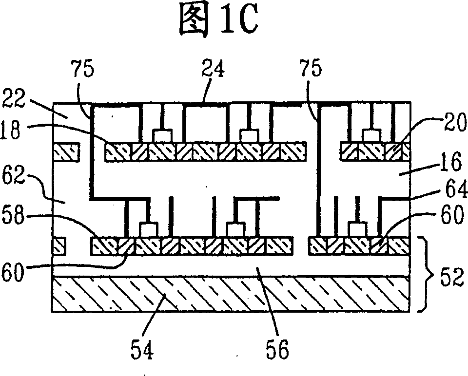
[0031] The present invention will be described in more detail below with reference to the accompanying drawings of the present invention. The present invention provides a three-dimensional integration scheme for fabricating three-dimensional CMOS integrated circuits with device layers formed on SOI wafers with different crystal orientations. In these drawings, similar reference numerals are used to designate similar and / or corresponding elements.

[0032] In the present invention, the term "silicon-on-insulator" or "SOI" wafer (the term "substrate" can be used interchangeably with the term "wafer") is used to define a semiconductor structure in which a buried oxide layer is used. The buried insulating layer separates the top silicon-containing layer (also called SOI layer or device layer) from the bottom silicon-containing substrate layer. The term "silicon-containing" is used in the present invention to mean a semiconductor material including silicon. Illustrative examples of such ...


PUM


Abstract

Three-dimensional (3D) integration schemes of fabricating a 3D integrated circuit in which the pFETs are located on an optimal crystallographic surface for that device and the nFETs are located on a optimal crystallographic surface for that type of device are provided. In accordance with a first 3D integration scheme of the present invention, first semiconductor devices are pre-built on a semiconductor surface of a first silicon-on-insulator (SOI) substrate and second semiconductor devices are pre-built on a semiconductor surface of a second SOI substrate. After pre-building those two structures, the structure are bonded together and interconnect through wafer-via through vias. In a second 3D integration scheme, a blanket silicon-on-insulator (SOI) substrate having a first SOI layer of a first crystallographic orientation is bonded to a surface of a pre-fabricating wafer having second semiconductor devices on a second SOI layer that has a different crystallographic orientation than the first SOI layer; and forming first semiconductor device on the first SOI layer.

Description

Technical field [0001] The present invention relates to a complementary metal oxide semiconductor (CMOS) integrated circuit, and more specifically to a three-dimensional CMOS integrated circuit with semiconductor device layers fabricated on wafers with different crystal orientations. Background technique [0002] In current semiconductor technology, CMOS devices such as nFET or pFET are typically manufactured on a semiconductor wafer having a single crystal orientation such as silicon. In particular, most of today's semiconductor devices are fabricated on silicon with (100) crystal orientation. [0003] It is known that electrons have high mobility in the (100) silicon surface orientation, but holes have high mobility in the (110) surface orientation. That is, the hole mobility on (100) silicon is about 2-4 times lower than the corresponding electron mobility in this crystal orientation. In order to compensate for this difference, pFETs are usually designed to have a larger width...

Claims


Application Information

Patent Timeline
Patent Type & Authority Patents(China)
IPC IPC(8): H01L21/82H01L21/84H01L21/8238H01L21/768H01L27/12H01L27/092H01L23/52H01L27/08H01L21/02H01L21/336H01L21/68H01L27/00H01L27/06H01L27/085H01L29/786
CPCH01L2924/0002H01L27/0688H01L21/6835H01L25/0657H01L27/1203H01L2221/68368H01L2924/00H01L27/085
Inventor 陈永聪凯瑟琳·W·瓜里尼杨美基
Owner GLOBALFOUNDRIES INC
Why Eureka
Try Eureka