Process for producing silicic coating, silicic coating and semiconductor device

a technology of silicic coating and semiconductor devices, applied in the direction of coatings, solid-state devices, basic electric elements, etc., can solve the problems of large influence of parasitic capacitance between lines, wire delay, and increased influence, and achieve easy production, increase the degree of crosslinking, and slow the effect of chemical reaction

Inactive Publication Date: 2013-04-30
FUJITSU LTD
View PDF28 Cites 2 Cited by
  • Summary
  • Abstract
  • Description
  • Claims
  • Application Information

AI Technical Summary

Benefits of technology

[0057]The silane compound of the invention encompasses compounds wherein the hydrogens on silanes (signifying compounds of the formula SinH2n+2), have been substituted with other groups, and compounds obtained by bonding such substituted compounds together through the substituents. The silane compound is not subject to any particular limitation, provided it has a photosensitive functional group; suitable use may be made of known compounds and derivatives thereof. The silane compound according to the invention may include impurities in a degree that does not interfere with the effects of the invention.
[0058]The photosensitive functional group of the invention is not subject to any particular limitation, provided it is a group which gives rise to a chemical reaction under irradiation with light, and may be suitably selected from among moieties that are known as photosensitive functional groups. Illustrative examples of such photosensitive functional groups include vinyl, acryloyl, benzyl, phenyl, carbonyl, carboxy, diazo, azido, cinnamoyl, acrylate, cinnamylidene, cyanocinnamylidene, furylpentadiene, p-phenylenediacrylate and pyridinyl groups. Of these, vinyl, phenyl and pyridinyl groups readily give rise to chemical reactions when irradiated with light, and are thus preferred.
[0059]The number of photosensitive functional groups included in a single molecule is not subject to any particular limitation. In general, a higher number of photosensitive functional groups is more advantageous because the degree of crosslinking increases accordingly. However, this is not always strictly the case as production becomes more difficult and drawbacks such as a slowing of the chemical reactions elicited by light irradiation also arise. For easy production, rapid chemical reactions upon irradiation with light, and facilitating an increase in the density of the film that has formed, the number of photosensitive functional groups which bond to a single atom of silicon on the silane compound is preferably at least two or more, and more preferably three.
[0060]The silicic coating precursor of the invention is a concept which encompasses everything from a film obtained using the silane compound of the invention to a film in the state immediately prior to formation of the silicic coating of the invention. That is, both films composed of the silane compound itself and films obtained by heating such a silane compound film and having an improved adherence to the workpiece (sometimes referred to herein simply as the “underlying material”) on which the silicic coating of the invention is to be formed are silicic coating precursors according to the present invention. The silicic coating precursor of the invention may be formed by any method. An illustrative example is a method wherein a solution of the silane compound of the invention dissolved in a solvent or, in cases where the silane compound of the invention is a liquid, the silane compound of the invention itself or a solution thereof is coated or sprayed onto the underlying material, then is heated or otherwise treated to remove the solvent. The coating method is not subject to any particular limitation and may be suitably selected according to the intended purpose. Illustrative examples include spin coating, dip coating, kneader coating, curtain coating and blade coating. Of these, from the standpoint of the ability to easily achieve a thin and uniform film, or the standpoint of coating efficiency or the like, a spin coating method is preferred. In the case of spin coating, exemplary conditions are a spinning rate of from about 100 to about 10,000 rpm, and preferably from 800 to 5,000 rpm, for a period of from about 1 second to about 10 minutes, and preferably from 10 to 90 seconds.
[0061]The solvent used is not subject to any particular limitation, provided it is capable of dissolving the silane compound of the invention and the solution has a good coatability. The solvent may be suitably selected from among known solvents. Illustrative examples of the solvent include methanol, ethanol, propanol, cyclohexanone, acetone, methyl isobutyl ketone, methyl ethyl ketone, methyl cellosolve, ethyl cellosolve, octane, decane, hexane, propylene glycol, propylene glycol monomethyl ether acetate, dioxane, diethyl ether, diethylene glycol, dimethyl sulfate, propylene glycol monomethyl ether, propylene glycol monoethyl ether, propylene glycol monopropyl ether and tetrahydrofuran. If the silane compound is a liquid, it may be acceptable to not use a solvent.
[0062]The silane compound of the invention preferably includes a compound represented by any one of general formulas (1) to (3) below, or includes a nitrogen-mediated compound obtained by removing at least one of X1, X2 and X3 from each of at least two compounds selected from the group consisting of compounds represented by any one of formulas (1) to (3) and bonding together the at least two compounds through nitrogen.

Problems solved by technology

This trend toward higher integration results in narrower line spacings, which has led to the problem of wire delay due to increased capacitance between lines {see Japanese Patent No. 3585384 (Paragraph No. 0002)}.
However, at line spacings of 1 μm or less, wire delay has an increased influence on device speed; in particular, when circuits are formed at line spacings of 0.1 μm or less, the parasitic capacitance between lines exerts a large influence on device speed.
When a barrier layer is not used in this case, thermal diffusion, etc. of the copper may result in copper infiltration into the silicon compound-based material, possibly causing the insulating properties of the low dielectric constant dielectric film to deteriorate.
This is an impediment to high-speed operation and high reliability in semiconductor integrated circuits.

Method used


Image

  • Process for producing silicic coating, silicic coating and semiconductor device
  • Process for producing silicic coating, silicic coating and semiconductor device
  • Process for producing silicic coating, silicic coating and semiconductor device

Examples


examples

[0078]Examples of the invention and comparative examples are described below.

examples 1 to 7

[0079](1) A porous silicon-containing dielectric film (an SiO2-like film containing primarily silicon and oxygen, and also containing carbon and hydrogen; Ceramate NCS, produced by JGC Catalysts and Chemicals, Ltd.) formed on a silicon substrate was produced.

[0080](2) Silane compound solutions prepared by mixing 0.1 mol of the respective silane compounds shown in Table 1 (corresponding to the “silane compound” of the invention) with 0.2 mol of methyl isobutyl ketone as the solvent were coated onto the porous silicic coating produced in (1) by spin coating at a spin rate of 2,000 rpm for a coating period of 30 seconds. The silicon substrate was then placed on a hot plate set at 100° C., and solvent drying was carried out for 1 minute.

[0081](3) Next, the porous silicon-containing dielectric films with the respective silicic coatings obtained in (2) were subjected to the light irradiation shown in Table 1. A high-pressure mercury-vapor lamp (wavelength, 200 to 600 nm) was used as the s...

examples 8 to 14

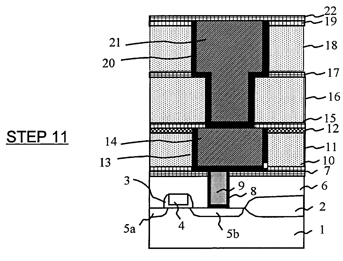
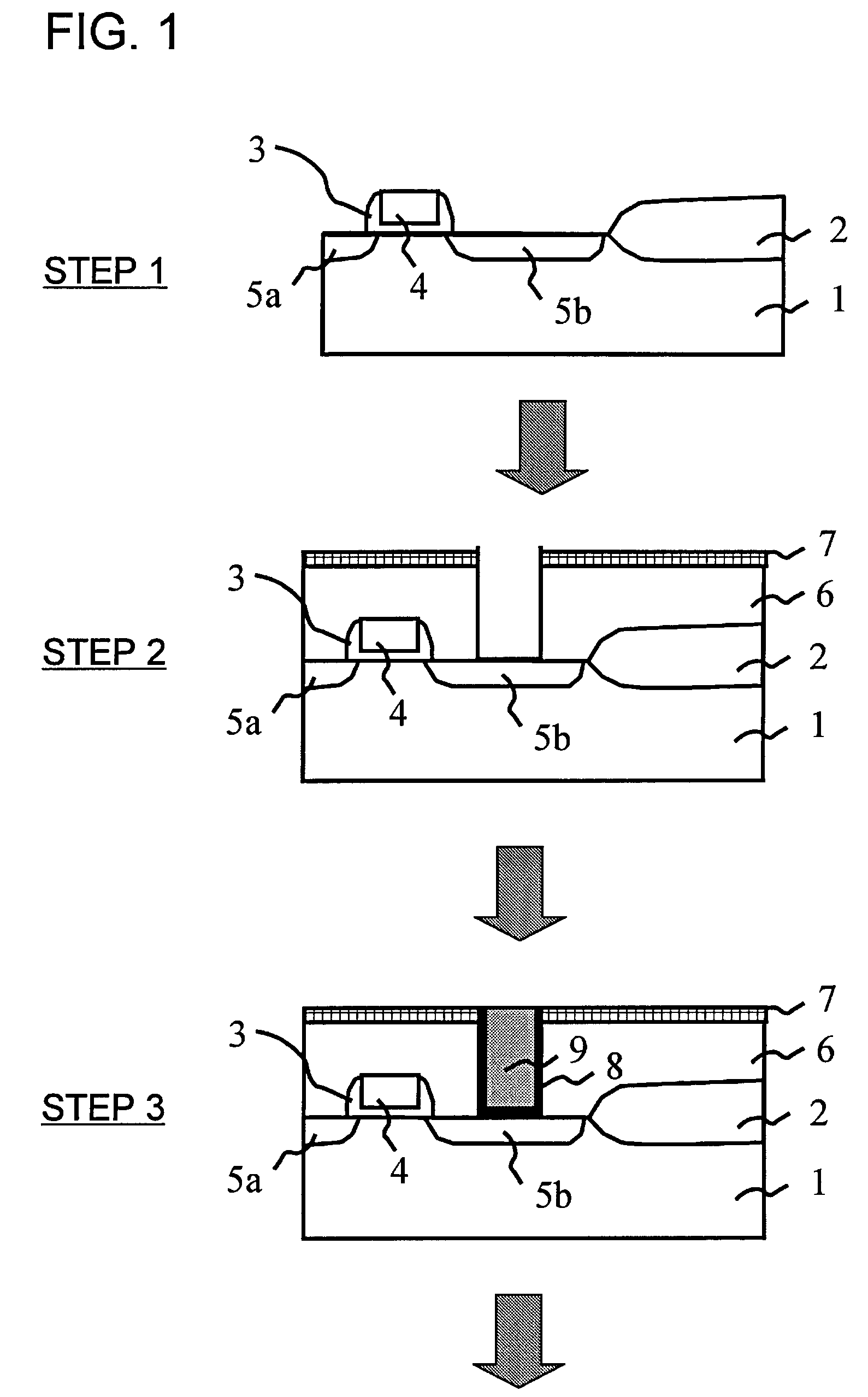
[0087](8) Referring to FIGS. 1 to 6, in Step 1, a silicon wafer 1 was isolated by an inter-device isolation film 2 and had formed thereon a transistor layer on which was formed a gate electrode having a source diffusion layer 5a, a drain diffusion layer 5b, and a sidewall dielectric film 3. In Step 2, an interlayer silicon dielectric 6 and a stopper film 7 were formed on the silicon wafer 1, and a contact hole for leading out an electrode was formed.

[0088]In Step 3, a TiN barrier metal film 8 was formed in the contact hole to a thickness of 50 nm by sputtering, following which a blanket of tungsten 9 was buried by mixing WF6 with hydrogen and reduction, then areas other than the via were removed by chemical mechanical polishing (CMP).

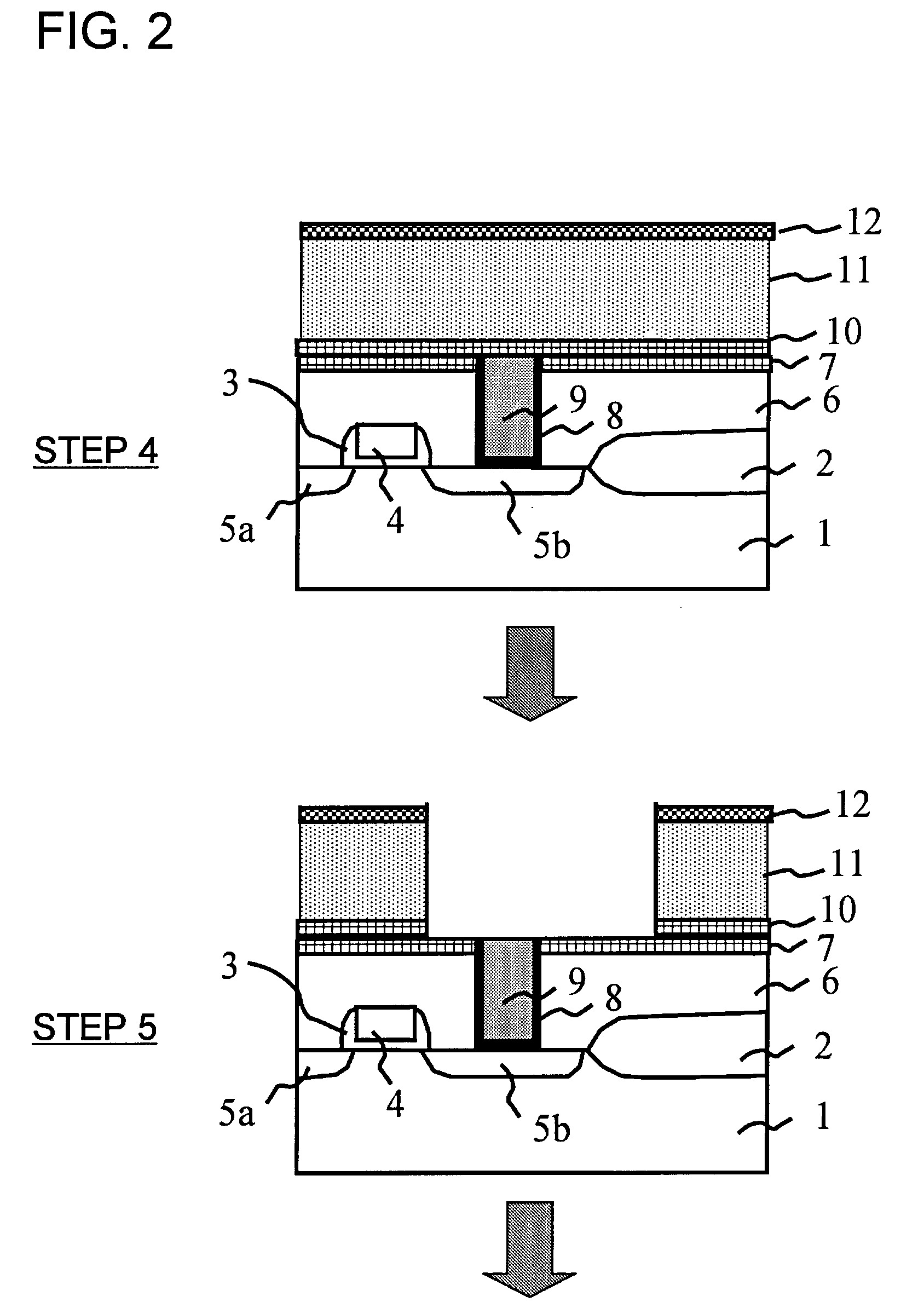
[0089]Next, in Step 4, a silane compound of the invention was coated, the solvent was removed by drying, then the applied coat was subjected to light irradiation to form a silicic coating 10 according to the present invention (silicic coatings according...


PUM

PropertyMeasurementUnit
densityaaaaaaaaaa
temperatureaaaaaaaaaa
wavelengthaaaaaaaaaa

Abstract

A silicic coating of 2.4 g / cm3 or higher density, obtained by forming a silicic coating precursor with the use of at least one type of silane compound having a photosensitive functional group and thereafter irradiating the silicic coating precursor with at least one type of light. This silicic coating can be used as a novel barrier film or stopper film for semiconductor device.

Description

CROSS-REFERENCE TO RELATED APPLICATIONS[0001]This application is a continuation of international application PCT / JP2007 / 000981, filed on Sep. 10, 2007.TECHNICAL FIELD[0002]The present invention relates to barrier films, stopper films and the like used in semiconductor devices.BACKGROUND OF THE INVENTION[0003]With the rising level of integration in semiconductor device integrated circuits and with higher device densities, there has been a growing demand for multilayer structures, particularly in semiconductor device elements. This trend toward higher integration results in narrower line spacings, which has led to the problem of wire delay due to increased capacitance between lines {see Japanese Patent No. 3585384 (Paragraph No. 0002)}.[0004]More specifically, although declines in signal propagation speed due to the parasitic capacitance of dielectric films have hitherto been known to occur, in generations of semiconductor devices with line spacings of more than 1 μm, wire delay had o...

Claims


Application Information

Patent Timeline
Patent Type & Authority Patents(United States)
IPC IPC(8): H01L21/76
CPCC09D183/04H01L21/02123H01L21/02216H01L21/02222H01L21/02282H01L21/02348H01L21/31144H01L21/3121H01L21/3125H01L21/3212H01L21/76829H01L23/5329H01L23/53295C08G77/20H01L2924/0002H01L21/76807H01L23/53238H01L2924/00
Inventor KOBAYASHI, YASUSHIYOSHIKAWA, KOUTANAKATA, YOSHIHIROIMADA, TADAHIROOZAKI, SHIROU
Owner FUJITSU LTD
Why Eureka
Try Eureka