Dopant diffusion modulation in GaN buffer layers

a technology of diffusion modulation and buffer layer, which is applied in the direction of basic electric elements, electrical equipment, semiconductor devices, etc., can solve the problems of affecting the conductivity of conventional gan transistors using mg doping in the buffer layer, difficult following the growth of mg doped materials, and residual mg continuing to contaminate the crystal for extended lengths of tim

Active Publication Date: 2013-04-30
EFFICIENT POWER CONVERSION CORP
View PDF11 Cites 25 Cited by
  • Summary
  • Abstract
  • Description
  • Claims
  • Application Information

AI Technical Summary

Benefits of technology

[0009]It would be desirable to provide a method and apparatus to achieve the improved breakdown of devices utilizing doped buffers, while eliminating the device performance variations caused by dopants near the barrier layer. To achieve this goal, it is desirable to trap excess dopants in order to avoid the above-mentioned disadvantages of the prior art.

Problems solved by technology

Growth of undoped GaN, with the intention of having material without Mg present, following the growth of Mg doped material is difficult due to the presence of Mg still residing on the surface of the GaN and other Mg on the walls of the chamber.
This residual Mg will continue to contaminate the crystal for extended lengths of time as Mg moves easily about the growth chamber.
In addition, conventional GaN transistors using Mg doping in the buffer layer suffer from changes in the conductivity caused by Mg near the barrier layer.

Method used


Image

  • Dopant diffusion modulation in GaN buffer layers
  • Dopant diffusion modulation in GaN buffer layers
  • Dopant diffusion modulation in GaN buffer layers

Examples


Embodiment Construction

[0014]In the following detailed description, reference is made to certain embodiments. These embodiments are described with sufficient detail to enable those skilled in the art to practice them. It is to be understood that other embodiments may be employed and that various structural, logical, and electrical changes may be made.

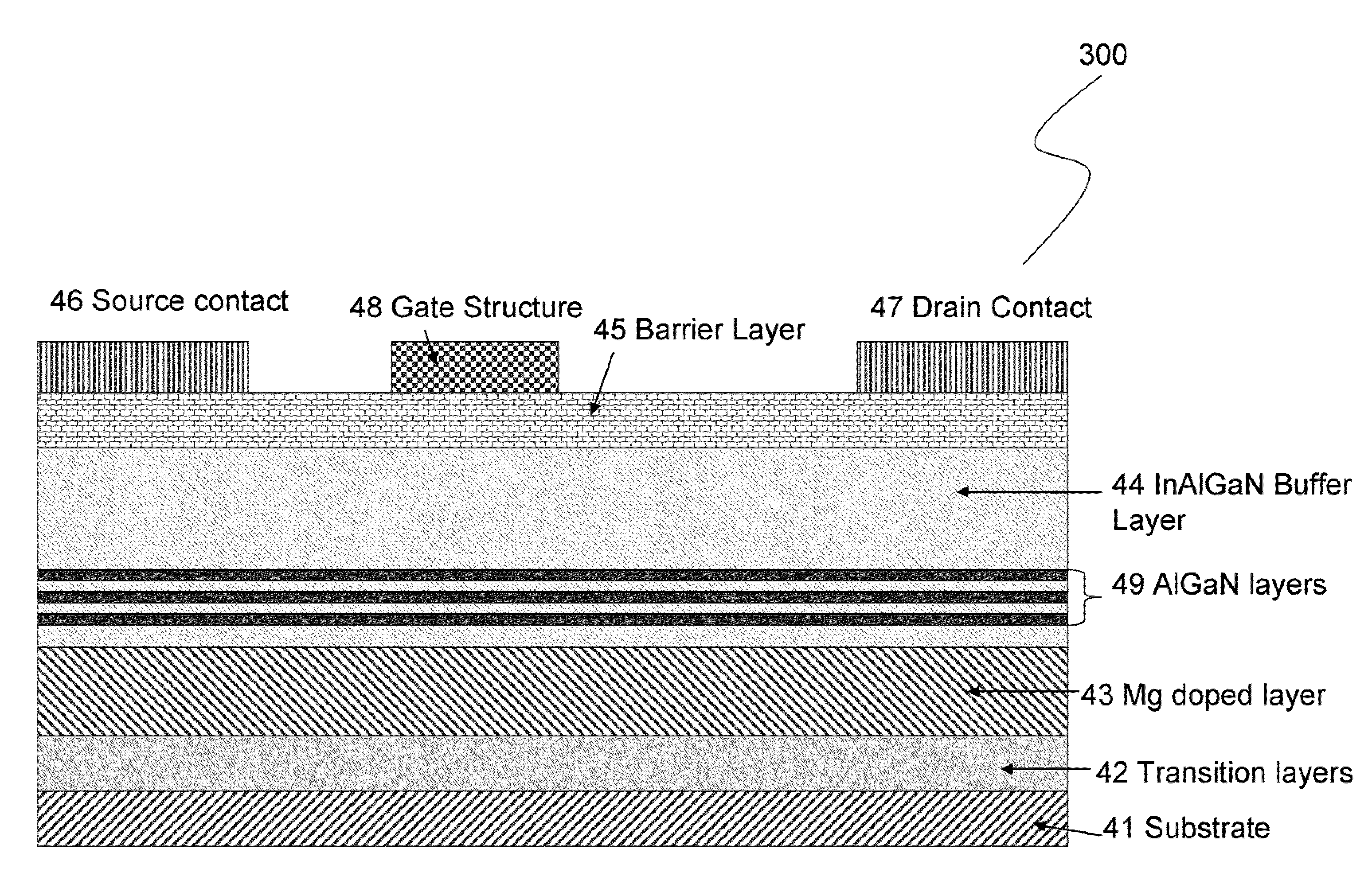
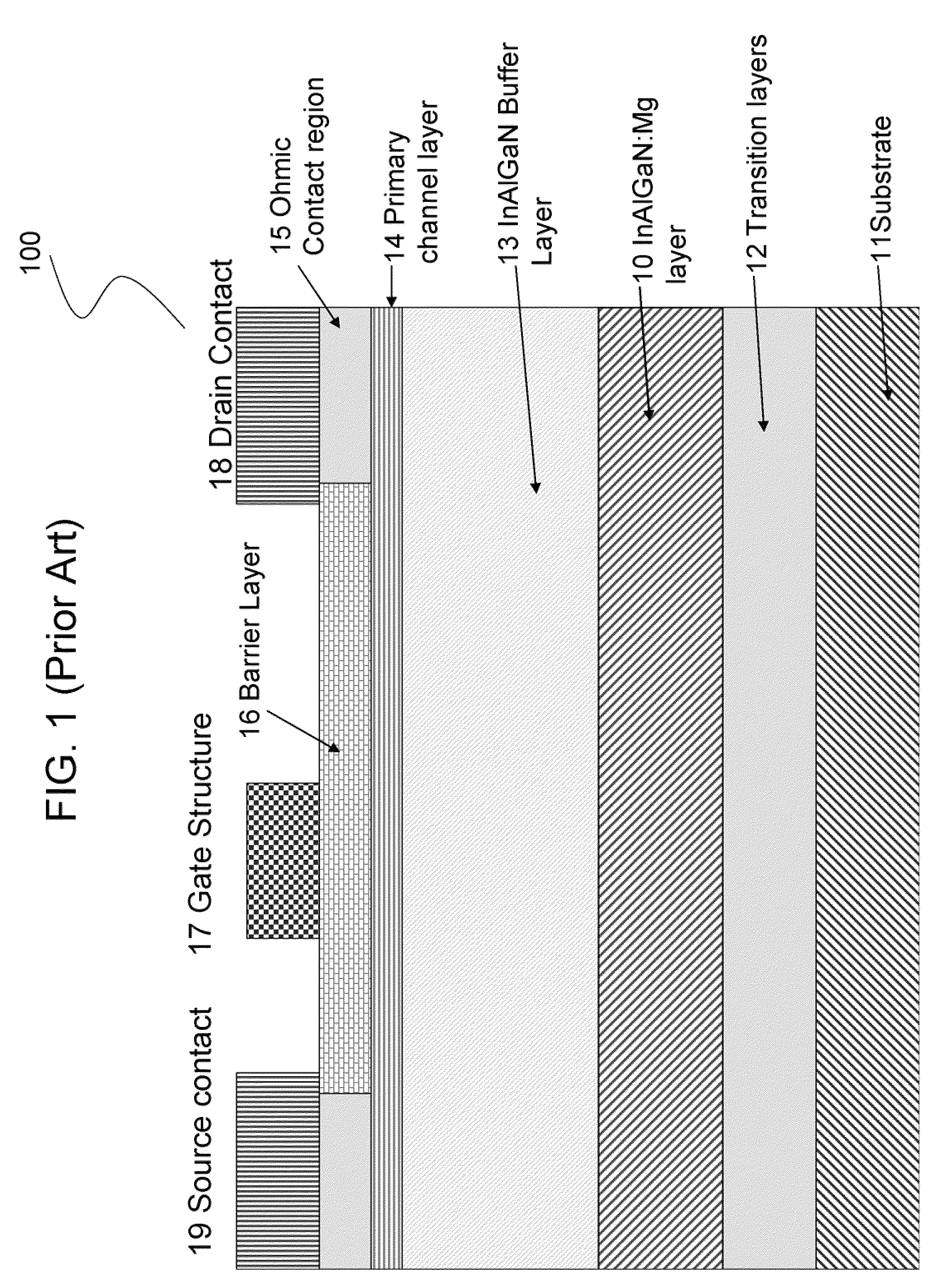
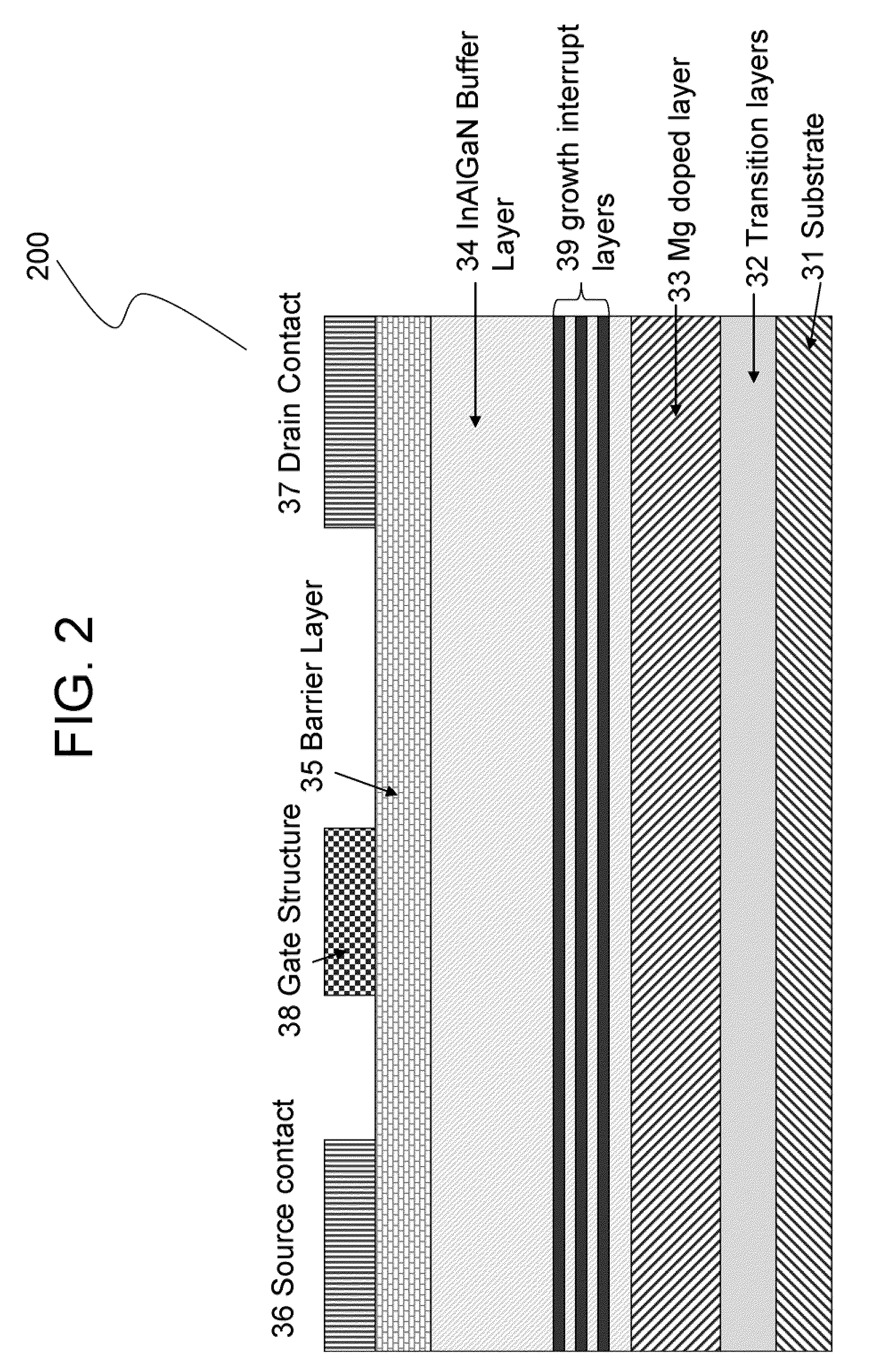
[0015]The present invention is a GaN transistor device with a Mg growth interruption layer to trap excess or residual dopants, and a method for making such a device. The invention is designed to force reaction of Mg with nitrogen, for example, to form a less volatile material, i.e., magnesium nitride. This material is then covered by a layer of either GaN or AlGaN. The coating step can be done at lower temperatures as well to assist the coating. By lowering the temperature, less reaction between the MgN and Al or Ga will occur. The reaction of Al and MgN is such that AlN is formed and MgN is reduced to Mg. This reaction is in competition with the desired coat...


PUM


Abstract

An enhancement mode gallium nitride (GaN) transistor with a Mg doped layer and a Mg growth interruption (diffusion barrier) layer to trap excess or residual Mg dopant. The Mg growth interruption (diffusion barrier) layer is formed by growing GaN, stopping the supply of gallium while maintaining a supply of ammonia or other nitrogen containing source to form a layer of magnesium nitride (MgN), and then resuming the flow of gallium to form a GaN layer to seal in the layer of MgN.

Description

CROSS REFERENCE TO RELATED APPLICATIONS[0001]This application claims priority from U.S. Provisional Application No. 61 / 167,820, filed on Apr. 8, 2009, which is hereby incorporated by reference in its entirety.FIELD OF THE INVENTION[0002]The present invention relates to the field of gallium nitride (GaN) transistors. In particular, the invention relates to a method and apparatus to trap excess dopants.BACKGROUND OF THE INVENTION[0003]Gallium nitride (GaN) semiconductor devices are increasingly desirable for power semiconductor devices because of their ability to carry large current and support high voltages. Development of these devices has generally been aimed at high power / high frequency applications. Devices fabricated for these types of applications are based on general device structures that exhibit high electron mobility and are referred to variously as heterojunction field effect transistors (HFET), high electron mobility transistors (HEMT), or modulation doped field effect tr...

Claims


Application Information

Patent Timeline
Patent Type & Authority Patents(United States)
IPC IPC(8): H01L29/66
CPCH01L21/0237H01L21/02439H01L21/02458H01L21/0254H01L21/02579H01L29/66462H01L29/7783H01L21/0262H01L29/207H01L29/452H01L29/2003H01L29/205
Inventor BEACH, ROBERTZHAO, GUANG YUAN
Owner EFFICIENT POWER CONVERSION CORP
Why Eureka
Try Eureka