Method of manufacturing semiconductor device

a manufacturing method and semiconductor technology, applied in semiconductor devices, solid-state devices, decorative arts, etc., can solve the problems of dispersion of chemical solutions, semiconductor substrate cracking, and dispersion of semiconductor substrates, so as to prevent chipping or cracking of semiconductor substrates.

Active Publication Date: 2013-05-07
MITSUBISHI ELECTRIC CORP
View PDF15 Cites 1 Cited by
  • Summary
  • Abstract
  • Description
  • Claims
  • Application Information

AI Technical Summary

Benefits of technology

[0015]The present invention has been made to solve the above-mentioned problems, and one object of the present invention is to provide a method of manufacturing a semiconductor device that suppresses chipping or cracking of a semiconductor substrate.
[0018]According to the former method of manufacturing a semiconductor device in accordance with the present invention, a protective film having a predetermined width from an outer peripheral end portion toward an inner side of a semiconductor substrate and extending along the outer peripheral end portion is formed on a first main surface of the semiconductor substrate. Thereby, when the ground second main surface is etched by discharging a predetermined chemical solution onto the second main surface with the second main surface facing upward, even if the chemical solution reaches the first main surface side of the outer peripheral end portion, the protective film extending along the outer peripheral end portion prevents the first main surface side from being etched. As a result, the outer peripheral end portion of the semiconductor substrate is inhibited from becoming like the edge of a knife, and chipping or cracking of the semiconductor substrate can be suppressed.
[0019]According to the latter method of manufacturing a semiconductor device in accordance with the present invention, a protective film having a predetermined width from an outer peripheral end portion toward an inner side of a semiconductor substrate and extending along the outer peripheral end portion is formed on a first main surface of the semiconductor substrate. Thereby, when the ground second main surface is etched by discharging a predetermined chemical solution onto the second main surface with the second main surface facing upward, even if the chemical solution reaches the first main surface side of the outer peripheral end portion, the first main surface side is prevented from being etched. As a result, the outer peripheral end portion of the semiconductor substrate is inhibited from becoming like the edge of a knife, and chipping or cracking of the semiconductor substrate can be suppressed. Further, since a semiconductor substrate with an outer peripheral end portion having been ground is prepared from the beginning, there is no need to grind the outer peripheral end portion of the semiconductor substrate.

Problems solved by technology

When a semiconductor substrate is worked to be thin by such a technique, distortion occurs in the semiconductor substrate.
However, since such treatment is performed after working the semiconductor substrate to be thin, there is a problem that the semiconductor substrate is likely to crack during the treatment.
With this technique, however, when wet etching treatment is performed on the rear surface of the semiconductor substrate to remove work distortion due to grinding or the like, a chemical solution may be scattered by the level difference at the outer peripheral end portion.
Further, when the semiconductor substrate is attached to a dicing frame in the step of dicing a wafer into individual chips, air bubbles may enter between the semiconductor substrate and a tape.
Furthermore, there is also a possibility that rear surface electrodes made of aluminum formed on the rear surface of the semiconductor substrate may be eroded when the level difference is removed, or that the yield of chips obtained may be decreased by providing the level difference.
In addition, reasons for causing the semiconductor substrate to crack easily include, in particular, that the outer peripheral end portion of the semiconductor substrate becomes like the edge of a knife.
Since the outer peripheral end portion of the semiconductor substrate is generally chamfered to have a cross section in the shape of a portion of an ellipse, the outer peripheral portion of the semiconductor substrate becomes like the edge of a knife when the semiconductor substrate is worked to be thin by polishing or the like, and thus the edge portion is likely to chip or crack.
This has caused a problem that the outer peripheral end portion of the semiconductor substrate is likely to chip or crack.

Method used


Image

  • Method of manufacturing semiconductor device
  • Method of manufacturing semiconductor device
  • Method of manufacturing semiconductor device

Examples


Embodiment Construction

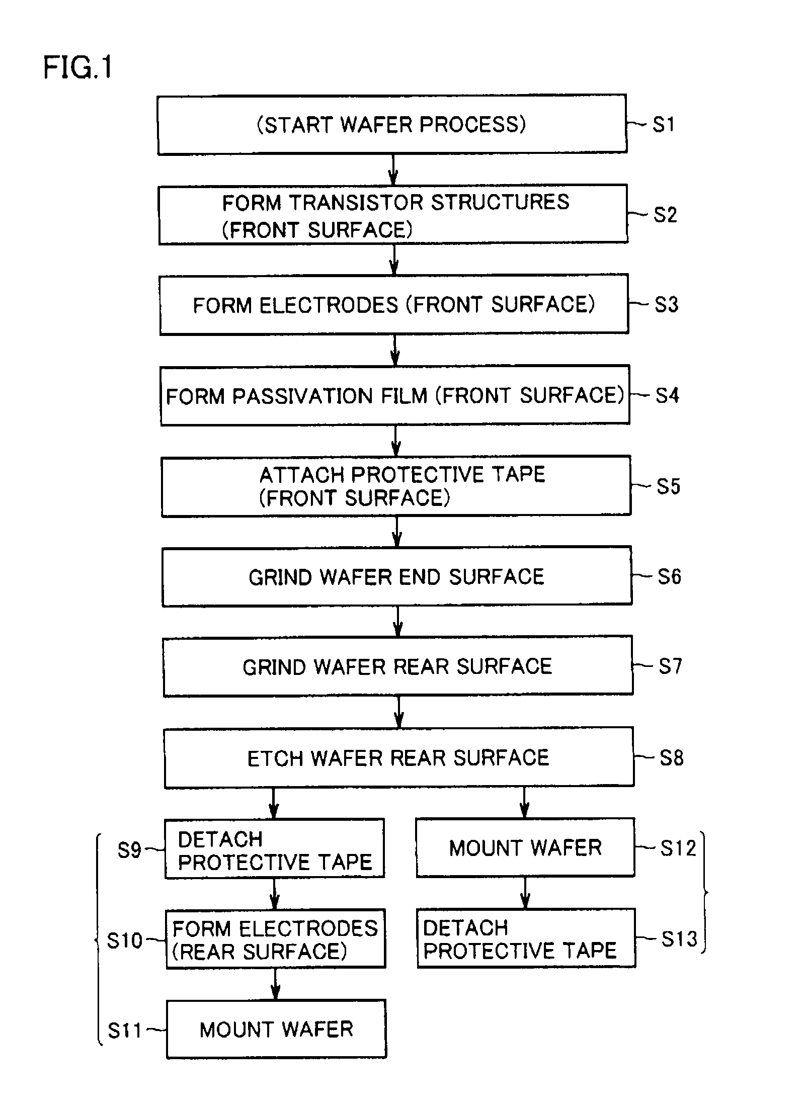
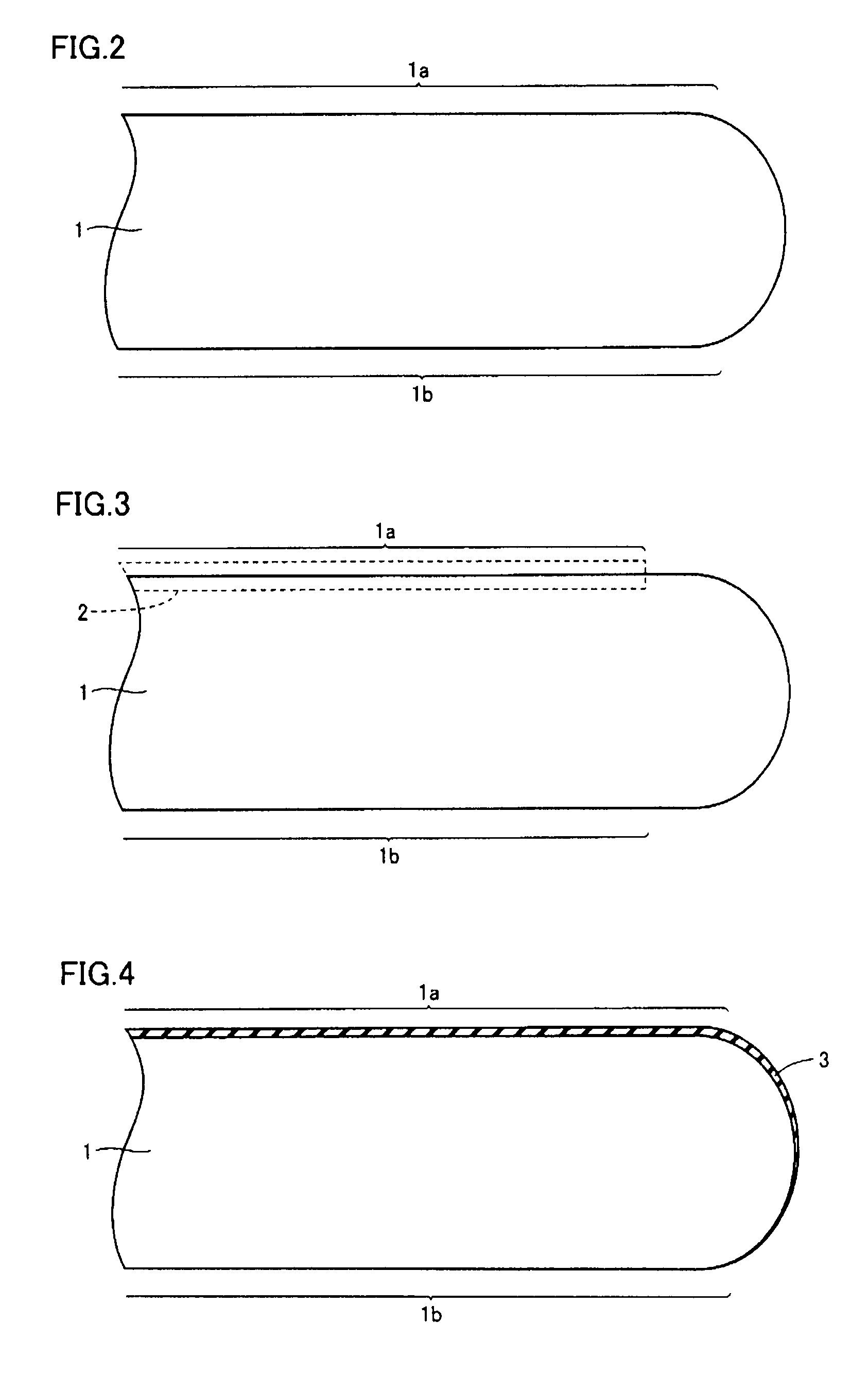
[0041]A method of manufacturing a semiconductor device in accordance with an embodiment of the present invention will be described. FIG. 1 shows a manufacturing flow of the semiconductor device. As shown in FIG. 1, firstly in step S1, a new semiconductor substrate (wafer) is prepared to start a wafer process. As shown in FIG. 2, at the time of starting a wafer process, an outer peripheral end portion of a semiconductor substrate 1 has a cross section in the shape of a portion of a circle or a portion of an ellipse.

[0042]Next, in step S2, as shown in FIG. 3, insulated gate structures, transistor devices, and the like are formed on a front surface 1a of semiconductor substrate 1 (within a dotted line frame 2) through a predetermined process. Then, in step S3, electrodes are formed in a predetermined region of front surface 1a of semiconductor substrate 1 (within dotted line frame 2). The electrodes are formed, for example, by forming an electrode material such as aluminum on front sur...


PUM

PropertyMeasurementUnit
thicknessaaaaaaaaaa
thicknessaaaaaaaaaa
thicknessaaaaaaaaaa

Abstract

A passivation film having a predetermined width from an outer peripheral end portion toward an inner side and extending along the outer peripheral end portion is formed on a front surface of a semiconductor substrate. An outer peripheral end surface orthogonal to the front surface and a rear surface is formed by grinding the outer peripheral end portion of the semiconductor substrate. A thickness of the semiconductor substrate is reduced to a predetermined thickness by grinding the rear surface. The ground rear surface is etched by discharging a mixed acid onto the rear surface while rotating the semiconductor substrate with the rear surface facing upward, to remove a fracture layer. Thereby, chipping or cracking of the semiconductor substrate is suppressed.

Description

BACKGROUND OF THE INVENTION[0001]1. Field of the Invention[0002]The present invention relates to a method of manufacturing a semiconductor device, and in particular, to a method of manufacturing a semiconductor device applied to a power device.[0003]2. Description of the Background Art[0004]In semiconductor devices, implementing a higher-density package by three-dimensional mounting or the like has been developed. Accordingly, reduction of a thickness of a wafer has been required, and the thickness of a wafer at the time of completion of a process for a semiconductor device has been reduced to a thickness of about 25 μm.[0005]Semiconductor devices include power devices such as an IGBT (Insulated Gate Bipolar Transistor) and an MOSFET (Metal Oxide Semiconductor Field Effective Transistor). These power devices (power semiconductor devices) are widely used, for example, as an inverter circuit for an industrial motor, an automotive motor, or the like, a power supply device for a large-c...

Claims


Application Information

Patent Timeline
Patent Type & Authority Patents(United States)
IPC IPC(8): B44C1/22
CPCH01L21/304H01L21/3083H01L21/6835H01L21/6836H01L2221/68327H01L2924/0002H01L2221/6834H01L2924/30105H01L2924/00
Inventor NAKATA, KAZUNARIMOTONAMI, KAORUNARAZAKI, ATSUSHIONOYAMA, AYUMUHONDA, SHIGETOFUJII, RYOICHIHIRATA, TOMOYA
Owner MITSUBISHI ELECTRIC CORP
Why Eureka
Try Eureka