Electro-optical device, shift register circuit, and semiconductor device

a technology of shift register and electronic device, applied in the field of electronic device, can solve the problem that the control electrode of the transistor b>204/b> is not sufficiently charged when the shift register is switched, and achieve the effect of preventing the rising speed of the gate line selection signal from decreasing

Active Publication Date: 2013-06-11
TRIVALE TECH LLC
View PDF16 Cites 29 Cited by
  • Summary
  • Abstract
  • Description
  • Claims
  • Application Information

AI Technical Summary

Benefits of technology

[0015]It is an object of the present invention to provide an electro-optical device capable of using a region of a gate line drive circuit efficiently and preventing the rising speed of a gate line selection signal from decreasing (rising delay), and a shift register circuit composed of a single conductivity type transistor which is suitable for the device.
[0018]According to the electro-optical device of the first and second aspects of the present invention, the odd and even drives are arranged so as to sandwich pixels, whereby the region of the scanning line drive circuit can be used efficiently. In addition, even in such a case, the output signal can be shifted without passing through a gate line. Therefore, the selection signal can be prevented from being delayed in rise because it is not affected by a resistance component and a capacitance component of the gate line.
[0021]According to the electro-optical device of the third and fourth aspects of the present invention, in each shift register circuit, the boosting unit allows the transistor charging the first node to operate in the unsaturated region. Accordingly, the voltage between the gate and the source of the first transistor can be further increased at high speed. Therefore, even when the frequency of the first clock signal is high, the driving capability of the first transistor, that is, the driving capability of the shift register circuit can be kept high, which contributes to higher speed operation. In addition, even when the odd and even drives are arranged so as to sandwich pixels to use the region of the scanning line drive circuit efficiently, the output signal can be shifted without passing through a gate line. Therefore, the selection signal can be prevented from being delayed in rise because it is not affected by a resistance component and a capacitance component of the gate line.
[0023]According to the shift register circuit of the present invention, since the second or third transistor charging the gate of the first transistor operates in the unsaturated region, the voltage between the gate and the source of the first transistor can be further increased at high speed. Therefore, even when the frequency of the first clock signal is high, the driving capability of the first transistor, that is, the driving capability of the shift register circuit can be kept high, which contributes to higher speed operation.
[0026]According to the semiconductor device of the present invention, the a-Si transistor serving as the MOS capacitor element can be high in gate capacitance functioning as the capacitor element and small in channel resistance while keeping its overlap capacitance between the gate and the drain low. Therefore, the power consumption of the MOS capacitor element can be cut and the response speed thereof can be increased.

Problems solved by technology

As a result, since charging speed of the control electrode of the transistor 204 slows down, there is a concern that the control electrode of the transistor 204 is not sufficiently charged when the shift register is operated at high speed.
This problem arises prominently in an electro-optical device having a long gate line such as a display device having a large screen.

Method used


Image

  • Electro-optical device, shift register circuit, and semiconductor device
  • Electro-optical device, shift register circuit, and semiconductor device
  • Electro-optical device, shift register circuit, and semiconductor device

Examples


first embodiment

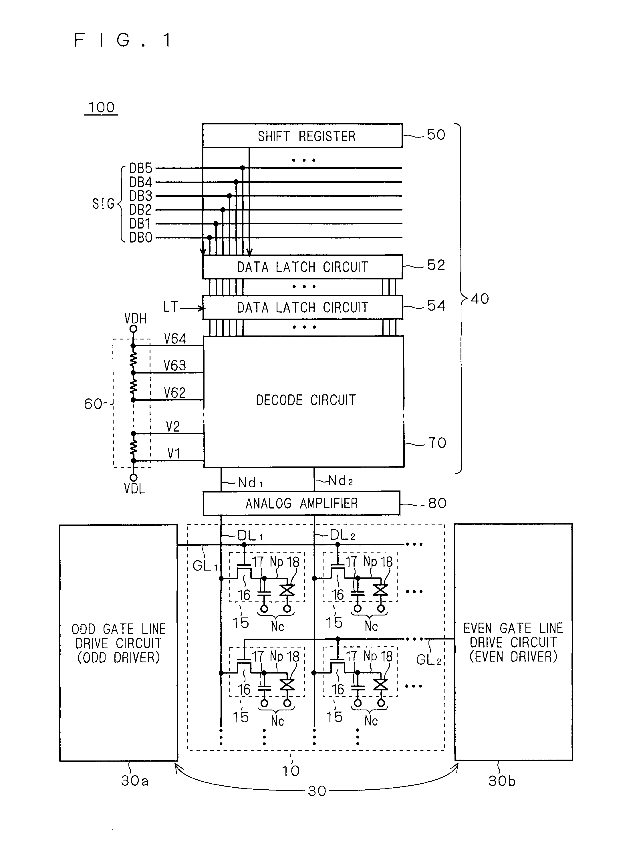
[0060]FIG. 1 is a schematic block diagram showing a configuration of a display device according to the present invention, and shows an entire configuration of a liquid crystal display device as a representative example of the display device. In addition, the present invention is not limited to the liquid crystal display device, and it may be widely applied to display devices to convert an electric signal to brightness of light, such as an electroluminescence (EL), organic EL, plasma display, and electronic paper, or electro-optical devices to convert intensity of light to an electric signal, such as an image capturing apparatus (imaging sensor).

[0061]A liquid crystal display device 100 includes a liquid crystal array section 10, a gate line drive circuit 30, and a source driver 40. The liquid crystal array section 10 includes a plurality of pixels 15 arranged in the form a matrix. Gate lines GL1, GL2 . . . (referred to as the “gate line GL” collectively) are provided for rows of the...

second embodiment

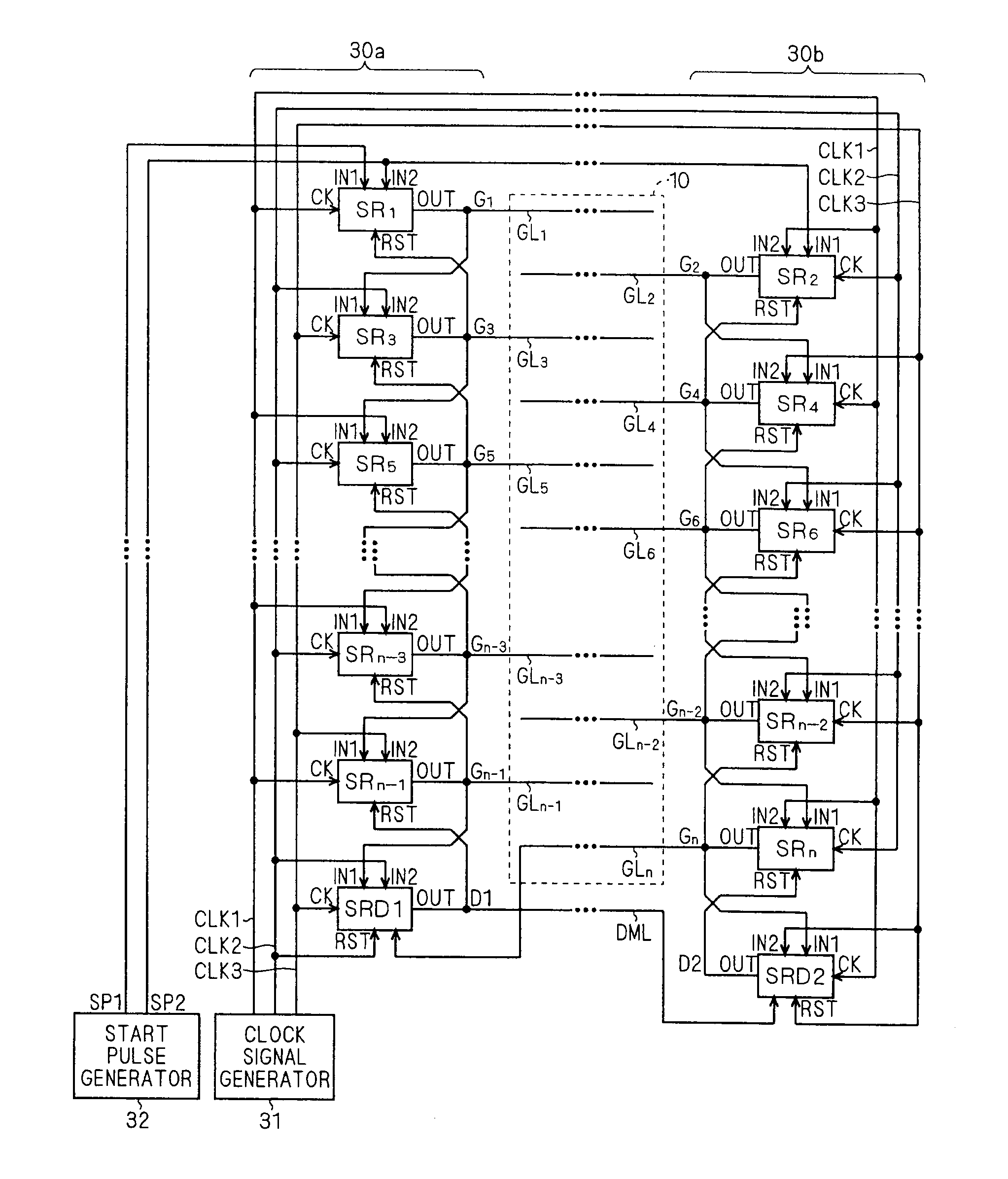
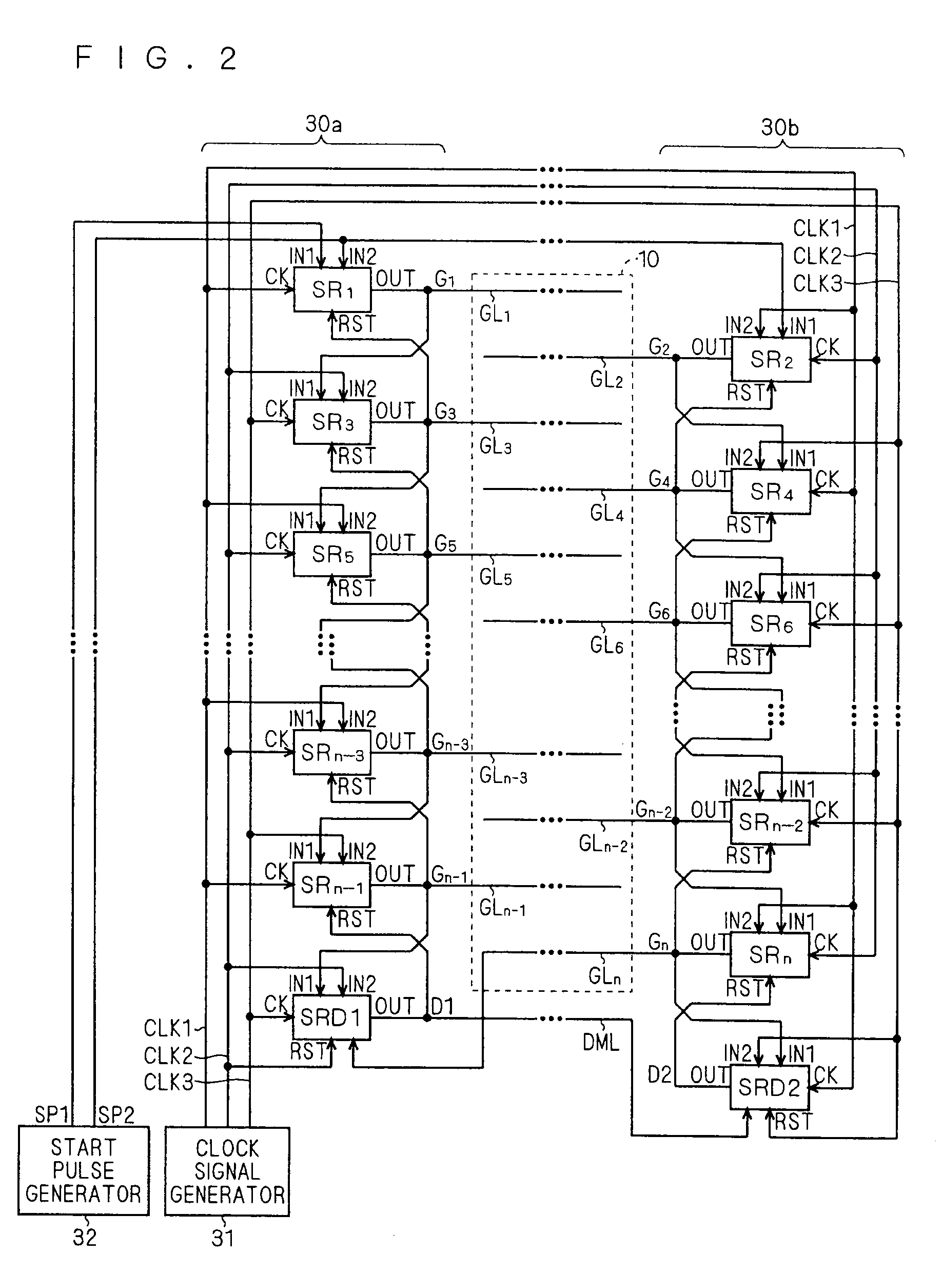
[0172]According to a second embodiment, a shift register capable of changing a shift direction of a signal is applied to the present invention. A gate line drive circuit 30 using such shift register is capable of bidirectional scanning. A direction from head to bottom (order of gate lines GL1, GL2, GL3 . . . ) is defined as a “forward direction”, and a direction from bottom to head (order of gate lines GLn, GLn−1, GLn−2 . . . ) is defined as a “backward direction”.

[0173]FIG. 12 is a drawing showing a configuration of the gate line drive circuit 30 according to the second embodiment. This gate line drive circuit 30 is also composed of an odd driver 30a having cascaded unit shift registers SR1, SR3, SR5 . . . to drive the gate lines GL1, GL3, GL5 . . . in the odd rows, and an even driver 30b having cascaded unit shift registers SR2, SR4, SR6 . . . to drive the gate lines GL2, GL4, GL6 . . . in the even rows.

[0174]In addition, control signals (first and second voltage signals Vn and Vr...

third embodiment

[0216]According to a third embodiment, the present invention is applied to a gate line drive circuit composed of unit shift registers SR capable of bidirectional scanning without using a switching circuit. Since a signal delay due to the switching circuit is not generated in each unit shift register, the same response speed as that of a usual unit shift register (performing only one directional shift) can be obtained. Such unit shift register is disclosed in Japanese Patent Application Laid-Open No. 2008-287753 according to the idea of the inventor of the present invention.

[0217]FIG. 14 is a circuit diagram of a unit shift register SRk according to the third embodiment, in which the present invention is applied to the circuit in FIG. 3 of Japanese Patent Application Laid-Open No. 2008-287753. The unit shift register SRk is also composed of an output circuit 20, a pull-up drive circuit 21, and a pull-down drive circuit 22, and the pull-up drive circuit 21 includes a forward pull-up d...


PUM


Abstract

An electro-optical device is configured to be capable of using a region of a gate line drive circuit efficiently and preventing rising speed of a gate line selection signal from decreasing (rising delay), and a shift register circuit is composed of a single conductivity type transistor which is suitable for the device. The gate line drive circuit including an odd driver to drive odd rows of a plurality of gate lines, and an even driver to drive even rows thereof. Each unit shift register in the odd and even drivers receives a selection signal in the second previous row and activates its own selection signal two horizontal periods later. A start pulse of the even driver is delayed in phase by one horizontal period with respect to a start pulse of the odd driver.

Description

BACKGROUND OF THE INVENTION[0001]1. Field of the Invention[0002]The present invention relates to an electro-optical device such as an image display device and an image capturing apparatus and more particularly, to a scanning line drive circuit only composed of a same conductivity type field-effect transistor, and a shift register circuit used therein.[0003]2. Description of the Background Art[0004]An electro-optical device having a scanning line drive circuit to scan pixels connected to a scanning line has been widely known. For example, an image display device (referred to as the “display device” hereinafter) such as a liquid crystal display device is configured such that a gate line (scanning line) is provided with respect to each pixel row (pixel line) of a display element (display panel) in which a plurality of pixels are arranged in a form of a matrix, and a display image is updated by sequentially selecting and driving the gate line every horizontal period of a display signal....

Claims


Application Information

Patent Timeline
Patent Type & Authority Patents(United States)
IPC IPC(8): G09G3/36
CPCG09G3/3677G11C19/28H01L29/78666H01L29/94G09G3/3611G11C27/04G09G2310/0267H01L29/7869
Inventor TOBITA, YOUICHI
Owner TRIVALE TECH LLC
Why Eureka
Try Eureka