Hall sensor for eliminating offset voltage

a technology of offset voltage and hall sensor, which is applied in the direction of instruments, galvano-magnetic devices, basic electric elements, etc., can solve the problems of inability to assign a shape and arrangement suitable for the respective functions, the offset voltage cannot be eliminated using spinning current, and the potential distribution of the element that generates the offset voltage, etc., to achieve the effect of enhancing the sensitivity of the hall element, reducing the size of the chip, and reducing the offset voltag

Inactive Publication Date: 2013-06-18
ABLIC INC
View PDF24 Cites 12 Cited by
  • Summary
  • Abstract
  • Description
  • Claims
  • Application Information

AI Technical Summary

Benefits of technology

[0022]Further, the Hall sensor according to the present invention is capable of eliminating an offset voltage by spinning current.
[0025]The use of the above-mentioned measures can eliminate the offset voltage by spinning current. Since the control current input terminals and the Hall voltage output terminals are arranged independently to each other, the input terminals can be formed larger while the output terminals can be formed smaller, to thereby enhance the sensitivity of the Hall element. Besides, since the above-mentioned effects can be achieved by a single Hall element, the chip size can be reduced.

Problems solved by technology

It is considered that an imbalanced potential distribution inside the element generates the offset voltage due to mechanical stress applied to the element from the outside or due to misalignment occurring in a manufacturing process.
However, in the first method, (JP 06-186103 A), if the currents, which are applied to the Hall sensing portion in two directions, or the output Hall voltages depend on the shape of the Hall element, the offset voltage cannot be eliminated utilizing spinning current.
Since each of the terminals alternately serves as the Hall voltage output terminal and the control current input terminal, it is impossible to assign a shape and an arrangement suitable for the respective functions.
As described above, the sensitivity and the offset voltage of the Hall element changes depending also on the shape and the arrangement of the four terminals, and hence there is a problem of how to select the shape and the arrangement of the terminals.
However, since a plurality of the Hall elements are used, there is a problem that the chip size increases, leading to an increase in cost.
In addition, the offset voltage elimination by the utilizing spinning current is insufficient to eliminate the offset voltage in some cases.

Method used


Image

  • Hall sensor for eliminating offset voltage
  • Hall sensor for eliminating offset voltage
  • Hall sensor for eliminating offset voltage

Examples


Embodiment Construction

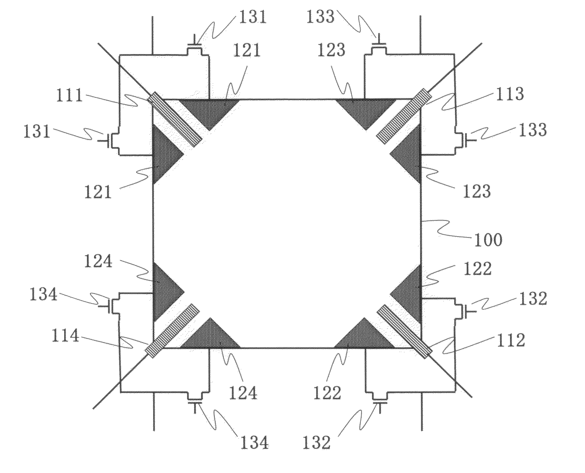
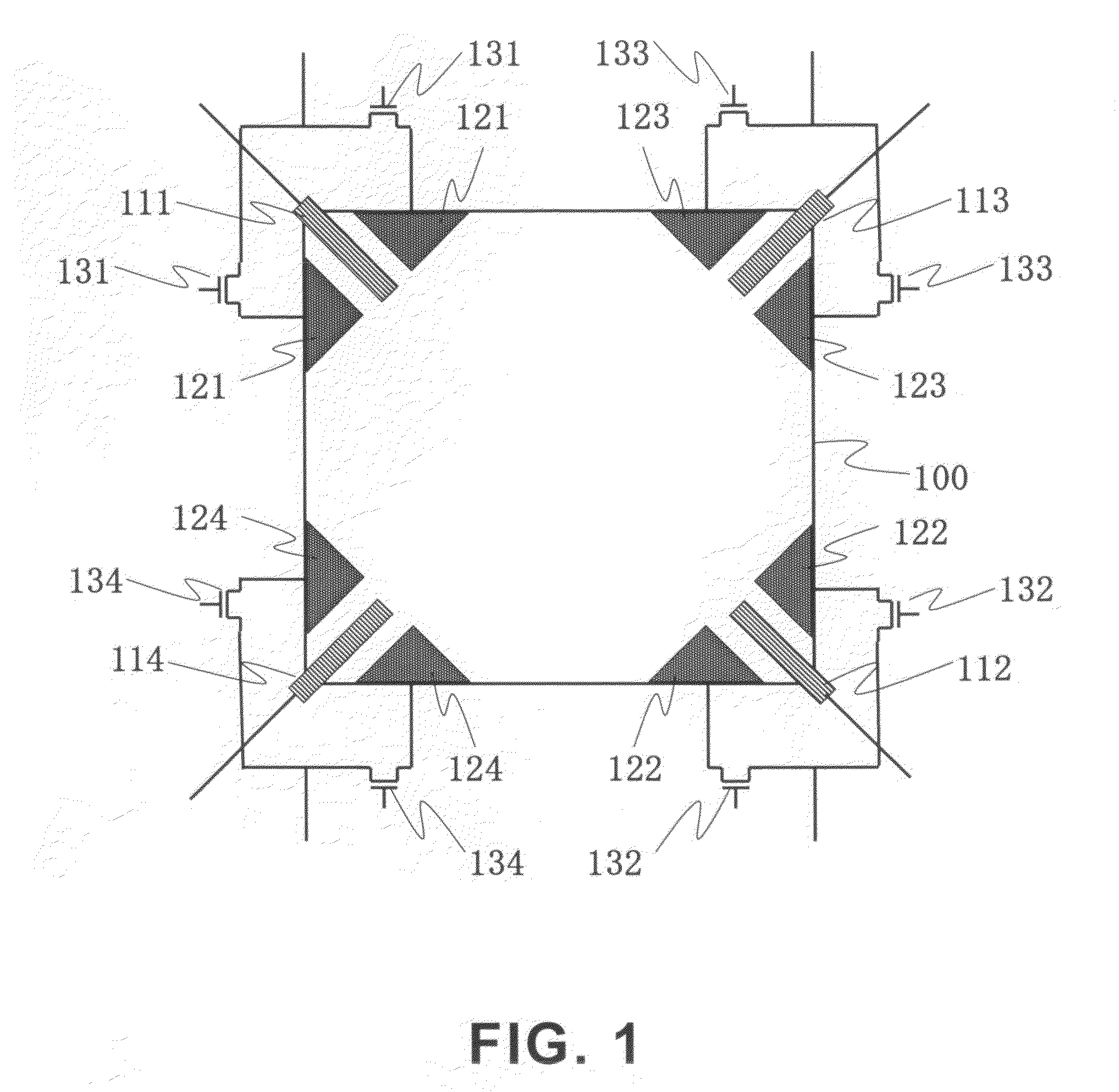
[0033]FIG. 1 is a plan view illustrating a structure of a Hall element according to an embodiment of the present invention. The Hall element of the present invention includes, at the four vertices of a Hall sensing portion 100 having a square shape, Hall voltage output terminals 111, 112, 113, and 114 and control current input terminals 121, 122, 123, and 124 which sandwich the Hall voltage output terminals, respectively. In other words, as the terminals connected to the Hall sensing portion, the Hall voltage output terminals and the control current input terminals are arranged as different independent terminals.

[0034]In the conventional method, the same terminal serves as both the Hall voltage output terminal and the control current input terminal, and hence in order to eliminate an offset voltage, the terminals having the two functions are all required to have the same shape. Each of the terminals alternately serves as the Hall voltage output terminal and the control current input...


PUM


Abstract

A Hall sensor has a P-type semiconductor substrate and a Hall sensing portion having a square shape and an N-type conductivity disposed on a surface of the semiconductor substrate. The Hall sensor includes Hall voltage output terminals having the same shape with each other, and control current input terminals having the same shape with each other. The Hall voltage output terminals are disposed at respective ones of four vertices of the Hall sensing portion. The control current input terminals include pairs of control current input terminals disposed at respective ones of the four vertices of the Hall sensing portion and arranged on both sides of respective ones of the Hall voltage output terminals in spaced apart relation from the Hall voltage output terminals so as to prevent electrical connection between the control current input terminals and the Hall voltage output terminals.

Description

BACKGROUND OF THE INVENTION[0001]1. Field of the Invention[0002]The present invention relates to a semiconductor Hall element, and more particularly, to a highly-sensitive Hall sensor capable of eliminating an offset voltage.[0003]2. Description of the Related Art[0004]At first, the principle for detecting magnetism of a Hall element is described. When a magnetic field is applied perpendicularly to a current flowing through a substance, an electric field, which causes a Hall voltage, is generated in a direction perpendicular to both the current and the magnetic field.[0005]Consider a Hall element illustrated in FIG. 2. When the width of a Hall sensing portion 1 which generates the Hall voltage according to the magnetic field is represented by W, the length thereof is represented by L, electron mobility thereof is represented by p, an applied voltage of a power source 2 for supplying a current is represented by Vdd, and an applied magnetic field is represented by B, the Hall voltage ...

Claims


Application Information

Patent Timeline
Patent Type & Authority Patents(United States)
IPC IPC(8): H01L29/82H01L23/58H01L43/00
CPCG01R33/07H01L43/065H10N52/101G01R15/202G01R33/075
Inventor HIOKA, TAKAAKIOMI, TOSHIHIKO
Owner ABLIC INC
Why Eureka
Try Eureka