Organic light emitting diode (OLED) device

a light-emitting diode and organic technology, applied in the direction of thermoelectric devices, organic semiconductor devices, discharge tube luminescent screens, etc., can solve the problems of reducing the intensity of electroluminescence of the oled device, deterioration of the materials of the organic layer, and large voltage rise over time,

Active Publication Date: 2013-07-02
AU OPTRONICS CORP
View PDF6 Cites 37 Cited by
  • Summary
  • Abstract
  • Description
  • Claims
  • Application Information

AI Technical Summary

Benefits of technology

[0008]The present invention, in one aspect, relates to an organic light emitting diode (OLED) device. In one embodiment, the OLED device includes a substrate, a cathode formed on the substrate, a first electroluminescent unit formed on the cathode, a charge generation layer (CGL) formed on the first electroluminescent unit, a second electroluminescent unit formed on charge generation layer, and an anode formed on the second electroluminescent unit. Each of the first and second electroluminescent units includes an electron-transport layer (ETL), an emission layer (EML) formed on the electron-transport layer, and a hole-transport layer (HTL) formed on the emission layer, such that the electron-transport layer of the first electroluminescent unit is formed on the cathode, defining a first energy barrier between the electron-transport layer of the first electroluminescent unit and the cathode, and the anode is formed on the hole-transport layer of the second electroluminescent unit, defining a second energy barrier between the hole-transport layer of the second electroluminescent unit and the anode, where the first energy barrier is higher than the second energy barrier. The first electroluminescent unit has a lifetime longer than that of the second electroluminescent unit.

Problems solved by technology

In particular, a critical problem with the inverted OLED exists in that voltage rise over time can be very large.
However, with the constant use and operation of the OLED devices, deterioration of the materials of the organic layers would decrease the intensity of electroluminescence of the OLED device.
This creates difficulties in achieving desired luminance.
Moreover, in color inverted OLED devices, materials for emitting lights in different colors would have different degrees of deterioration within the same operation time.
Thus, the lifetime of the electroluminescent units of the inverted OLED devices would be different, which results in color shift after long operation time of the OLED devices.
Therefore, a heretofore unaddressed need exists in the art to address the aforementioned deficiencies and inadequacies.

Method used


Image

  • Organic light emitting diode (OLED) device
  • Organic light emitting diode (OLED) device
  • Organic light emitting diode (OLED) device

Examples


Embodiment Construction

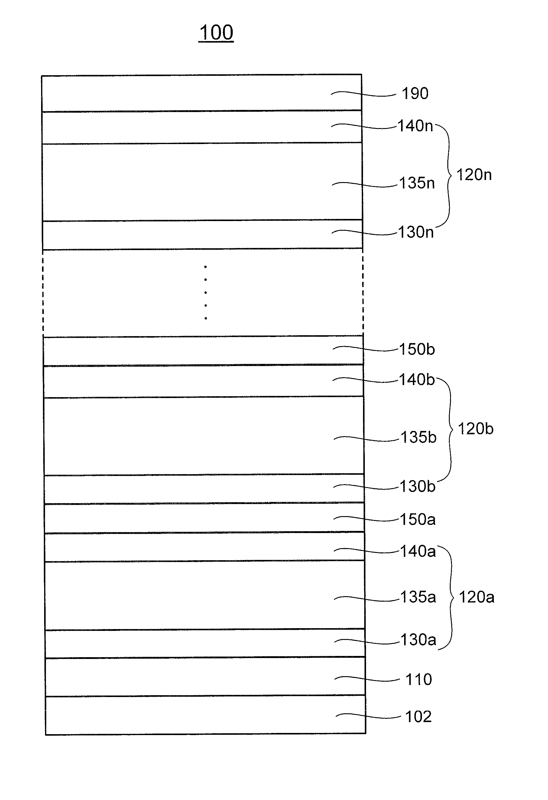
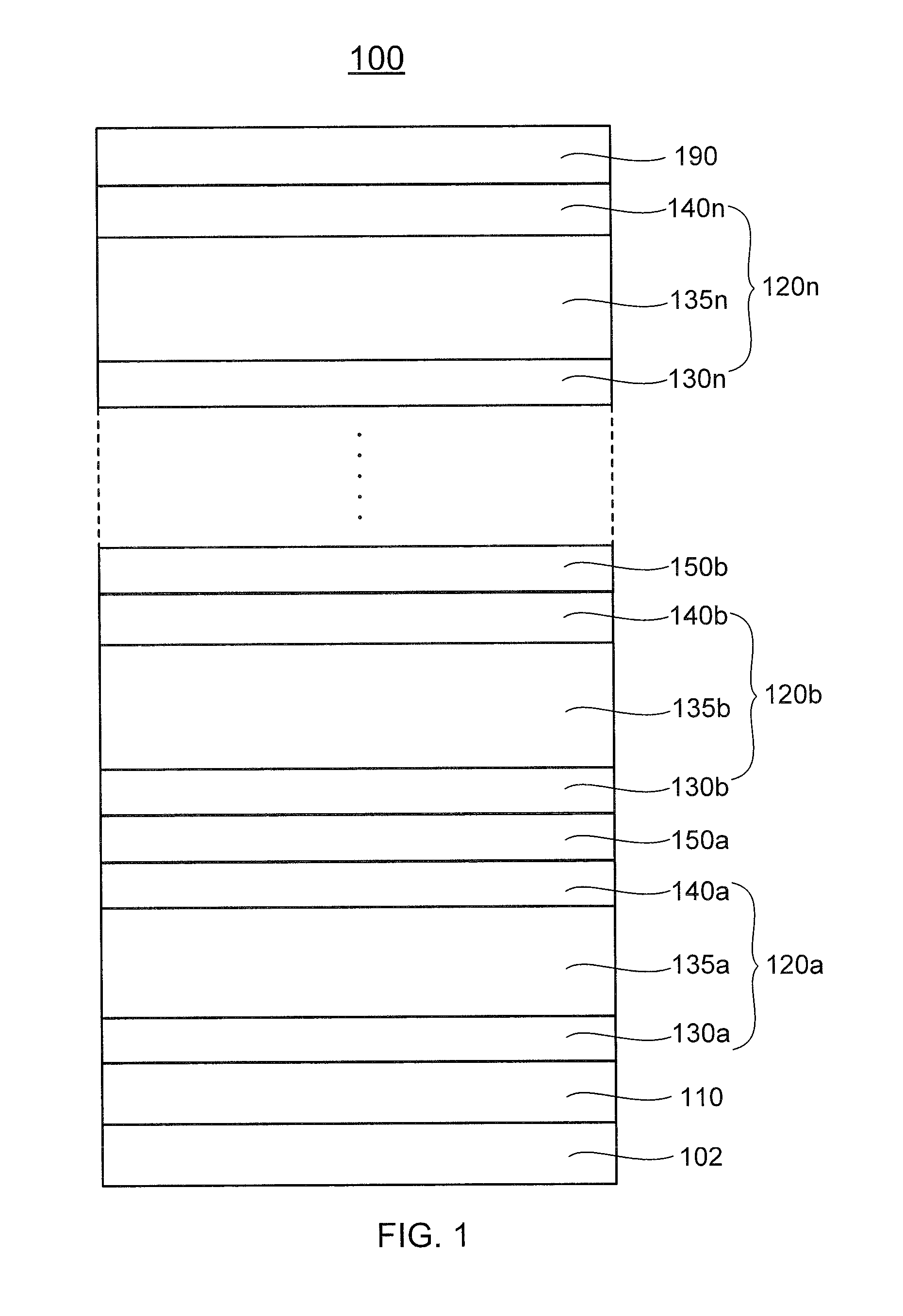
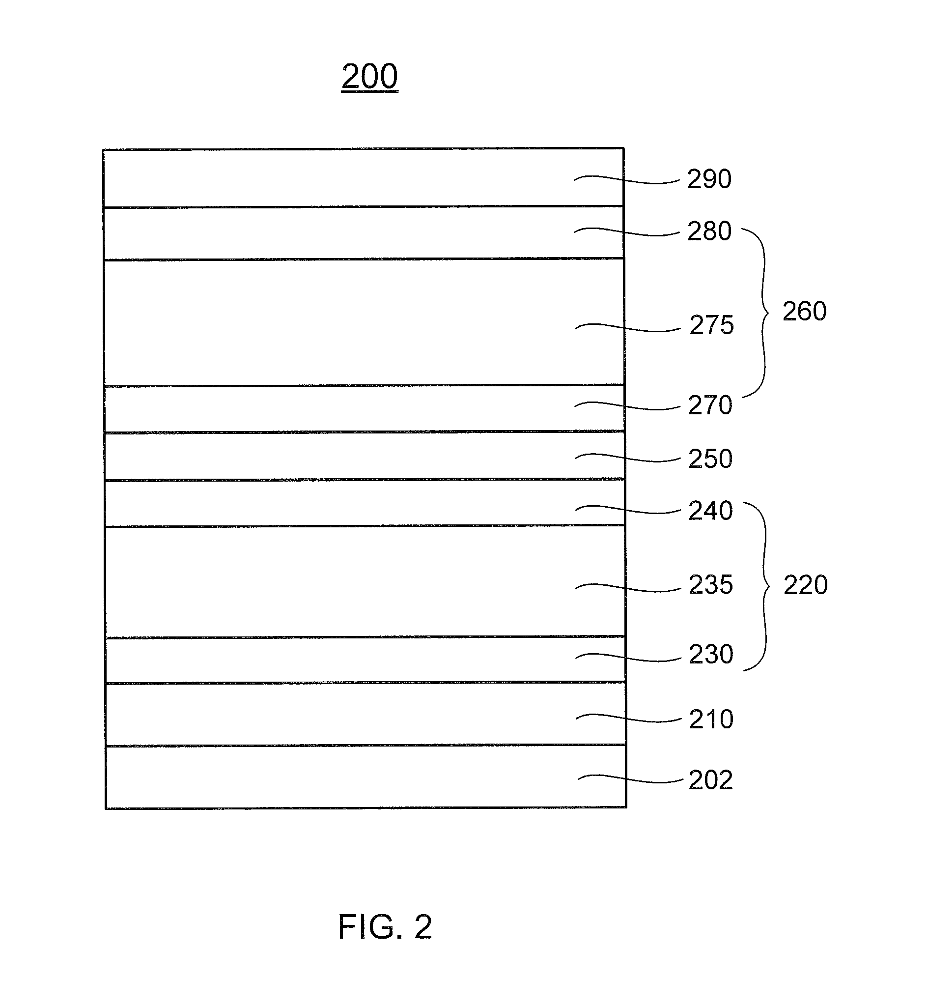
[0041]The present invention will now be described more fully hereinafter with reference to the accompanying drawings, in which exemplary embodiments of the invention are shown. This invention may, however, be embodied in many different forms and should not be construed as limited to the embodiments set forth herein. Rather, these embodiments are provided so that this disclosure will be thorough and complete, and will fully convey the scope of the invention to those skilled in the art. Like reference numerals refer to like elements throughout.

[0042]The terms used in this specification generally have their ordinary meanings in the art, within the context of the invention, and in the specific context where each term is used. Certain terms that are used to describe the invention are discussed below, or elsewhere in the specification, to provide additional guidance to the practitioner regarding the description of the invention. For convenience, certain terms may be highlighted, for examp...


PUM


Abstract

In one aspect of the invention, an organic light emitting diode device has a substrate, a cathode formed on the substrate, an anode spaced-apart from the cathode, a plurality of electroluminescent units stacked between the cathode and the anode, and a plurality of charge generation layers, each of which is formed between two adjacent electroluminescent units. Each electroluminescent unit has an electron-transport layer, an emission layer formed on the electron-transport layer, and a hole-transport layer formed on the emission layer. The electron-transport layer of the first electroluminescent unit is formed on the cathode, defining a first energy barrier, and the anode is formed on the hole-transport layer of the last electroluminescent unit, defining a second energy barrier. The first energy barrier is higher than the second energy barrier. The first electroluminescent unit has a lifetime longer than that of each of the rest electroluminescent units.

Description

FIELD OF THE INVENTION[0001]The present invention relates generally to an organic light emitting diode (OLED), and more particularly, to a color-stable inverted tandem OLED device.BACKGROUND OF THE INVENTION[0002]OLED devices have drawn great attention in display industries, and particularly in the flat-panel display industry, because it is operable with a low driving voltage and capable of generating light of red, green, and blue colors with high luminance efficiency. These unique attributes are derived from a basic OLED structure comprising of a multilayer stack of thin films of small-molecule organic materials sandwiched between an anode and a cathode. Typically, OLED devices are fabricated in forward-stacked structures with the anode placed in contact with the substrate or support on which the OLED is constructed, and the cathode placed on the top of the OLED.[0003]Low power consumption displays typically use an active matrix backplane where thin film transistors (TFT made of a-...

Claims


Application Information

Patent Timeline
Patent Type & Authority Patents(United States)
IPC IPC(8): H01L51/52
CPCH01L51/5004H01L27/3209H01L51/506H01L51/5076H01L51/5221H01L51/5278H01L2251/5353H01L2251/5376H10K59/32H10K50/11H10K2101/40H10K50/155H10K50/165H10K50/82H10K50/19H10K2102/321H10K2101/27
Inventor WU, CHANG-YENCHO, TING-YILEE, MENG-TINGHO, MENG-HUANCHIANG, PO-HSUANCHEN, CHIEH-WEI
Owner AU OPTRONICS CORP
Why Eureka
Try Eureka