

Modeling circuit cells for waveform propagation
a circuit cell and waveform propagation technology, applied in the field of circuit cell timing analysis and signal intengrity analysis, can solve problems such as voltage waveform distortion, logic transition errors, timing violations in other parts of the design,
- Summary
- Abstract
- Description
- Claims
- Application Information
AI Technical Summary
Benefits of technology
Problems solved by technology
Method used
Image

Examples
Embodiment Construction
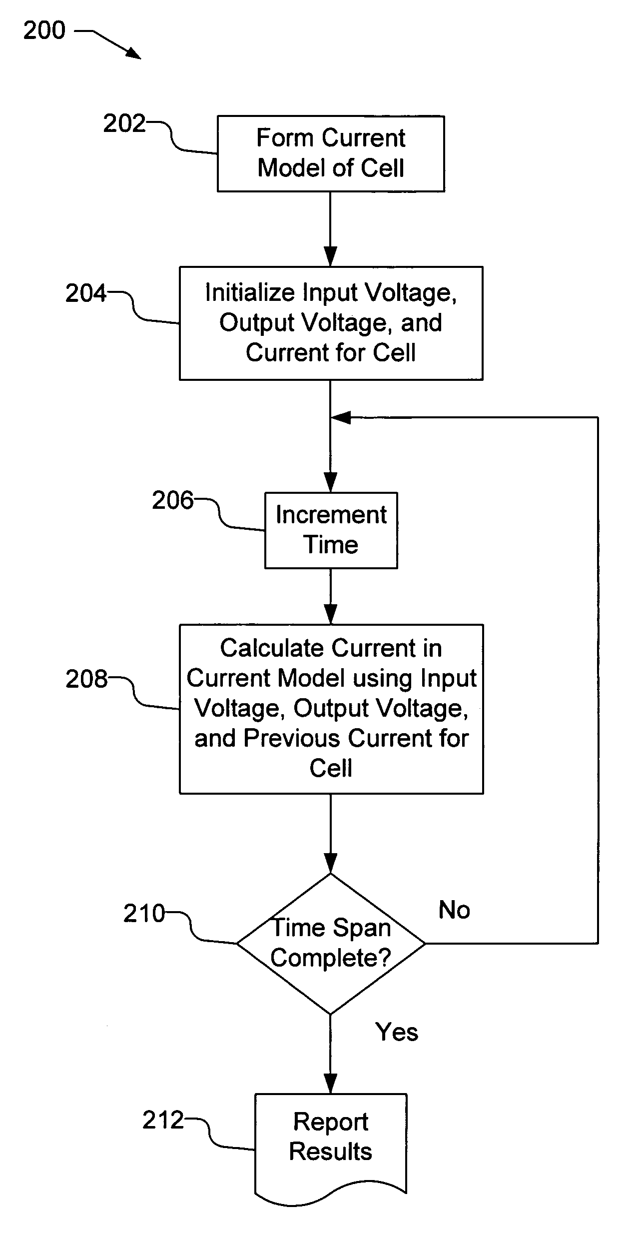
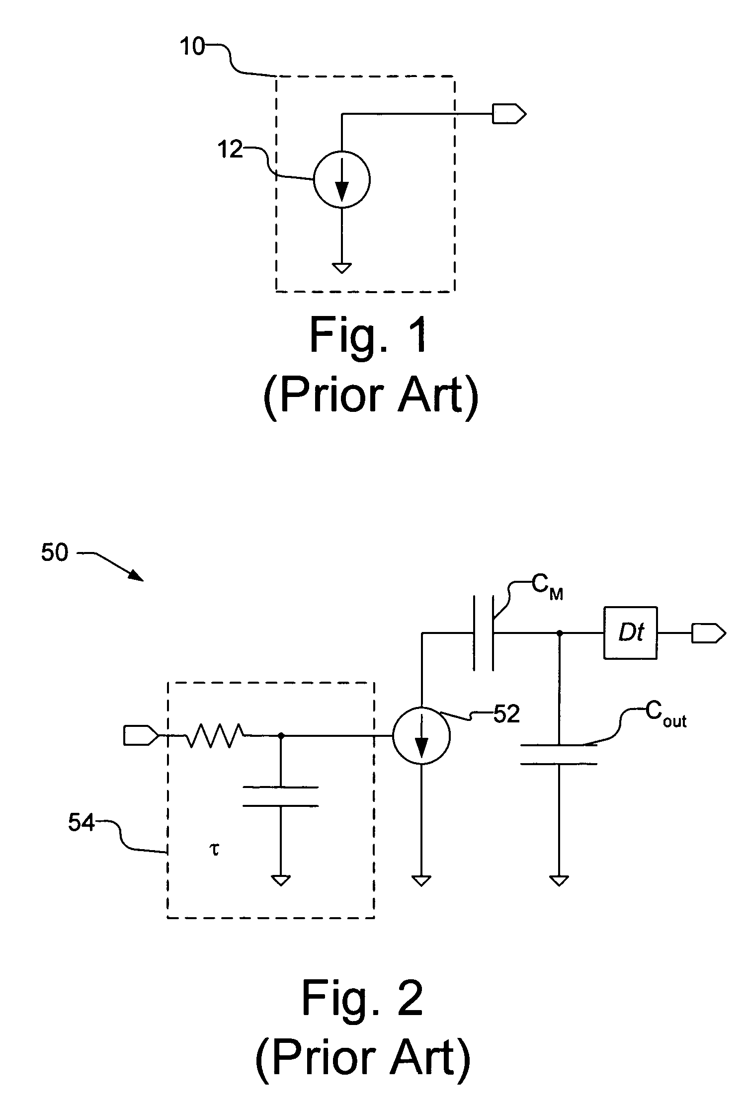
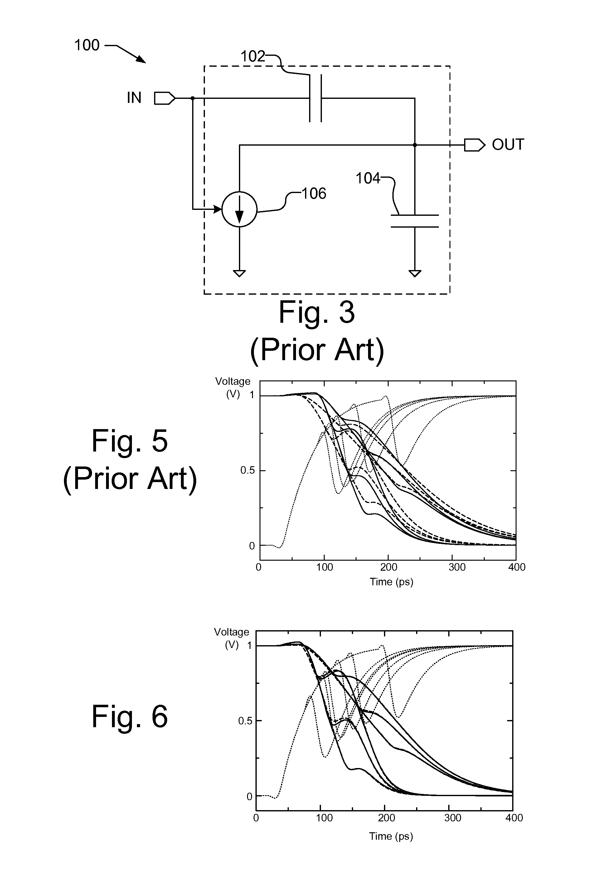
[0020]FIG. 3 schematically illustrates a current model 100 of a circuit cell that is used in accordance with an embodiment of the present invention. The current model 100 may include a Miller capacitor 102 between the input terminal IN and output terminal OUT, an output terminal capacitor 104 and a current source 106. The current of the current source 106 is a function of the cell input voltage, cell output voltage, and in one embodiment, the history of the cell current. The current history may be calculated as an integral of weighted past currents. The use of current history, input voltage, and output voltage with the current model 100 has been found to be suitable for all signal integrity analysis including, but not limited to, crosstalk delay, noise propagation, driver weakening, and combined noise propagation and noise injection.
[0021]Conventionally, the current model 100 is used as a static Vin-Vout indexed lookup table. The current that is drawn from current source 106 is conv...
PUM
 Abstract
Description
Claims
Application Information