Wafer level packaging method of encapsulating the bottom and side of a semiconductor chip

a technology of semiconductor chips and packaging methods, applied in semiconductor devices, semiconductor/solid-state device details, electrical devices, etc., can solve the problems of complex production process, achieve simple and feasible production process, reduce the thickness of semiconductor chips, and reduce the effect of thickness

Active Publication Date: 2013-07-16
ALPHA & OMEGA SEMICON INC
View PDF1 Cites 9 Cited by
  • Summary
  • Abstract
  • Description
  • Claims
  • Application Information

AI Technical Summary

Benefits of technology

[0017]The double-sided tape has good ductility, such that, after the whole semiconductor chip is flipped and attached on top surface of the double-sided tape, it can stretch to enlarge the space between the adjacent chip packages for the deposition of the molding compound into this space. The bottom surface of the double sided tape is attached on the supporting substrate to maintain the space between the adjacent chip packages. The dicing film can be a UV tape. The double-sided tape can be a thermal release tape or UV release tape. The supporting substrate can be a glass substrate or other semiconductor substrates.
[0018]Compared with the existing technologies, the wafer level packaging method in this invention provides a chip package structure with the side and bottom of the semiconductor chip encapsulated by a molding compound through a simple and feasible production process.

Problems solved by technology

However, the production process is very complicated.

Method used


Image

  • Wafer level packaging method of encapsulating the bottom and side of a semiconductor chip
  • Wafer level packaging method of encapsulating the bottom and side of a semiconductor chip
  • Wafer level packaging method of encapsulating the bottom and side of a semiconductor chip

Examples


Embodiment Construction

[0024]A number of embodiments of this invention will be described as follows with illustration drawings.

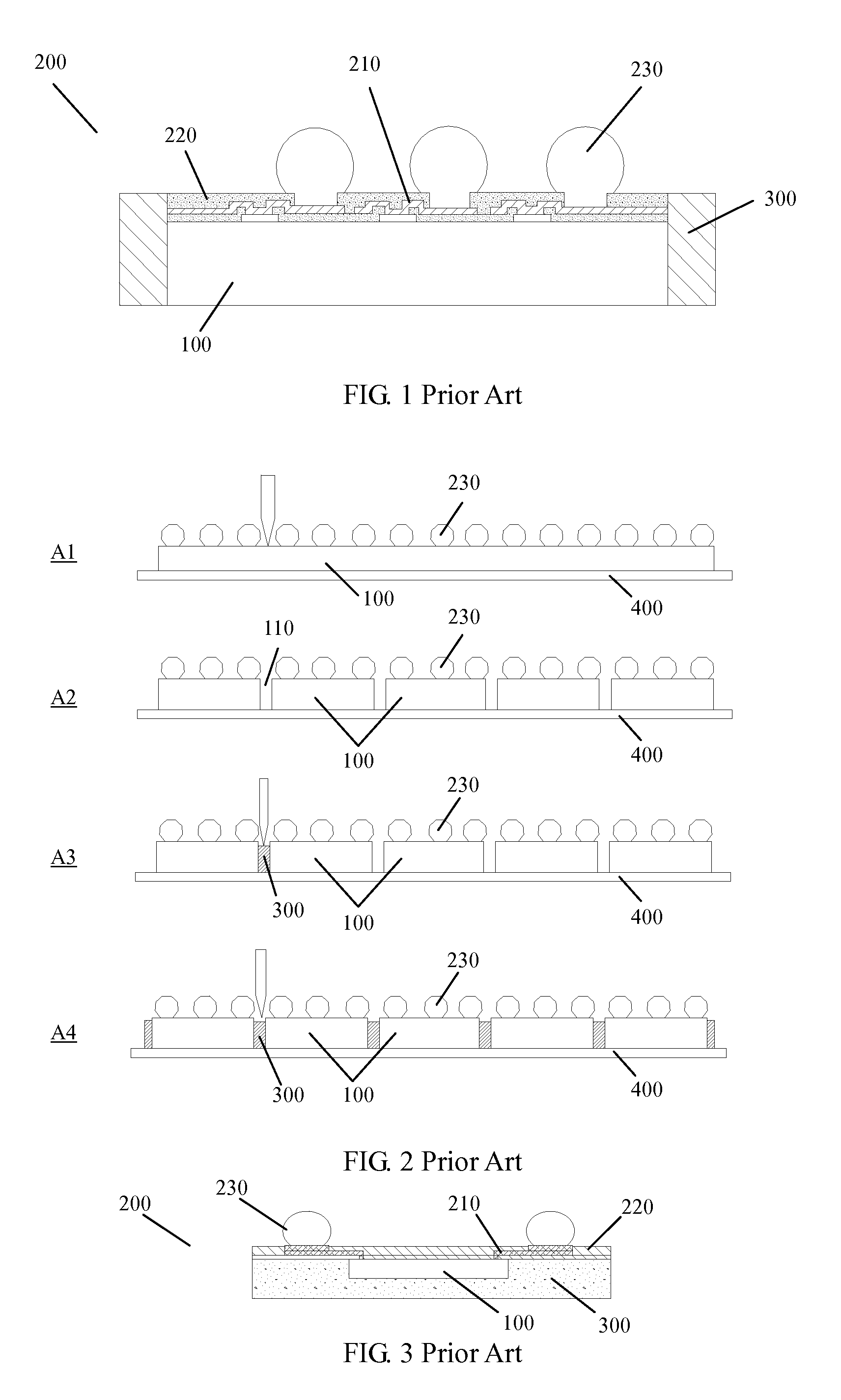
[0025]The wafer level packaging method in this invention is especially suitable for the encapsulating of MOSFET or other similar semiconductor chips, so that the bottom and side of each semiconductor chip are protected with a molding compound.

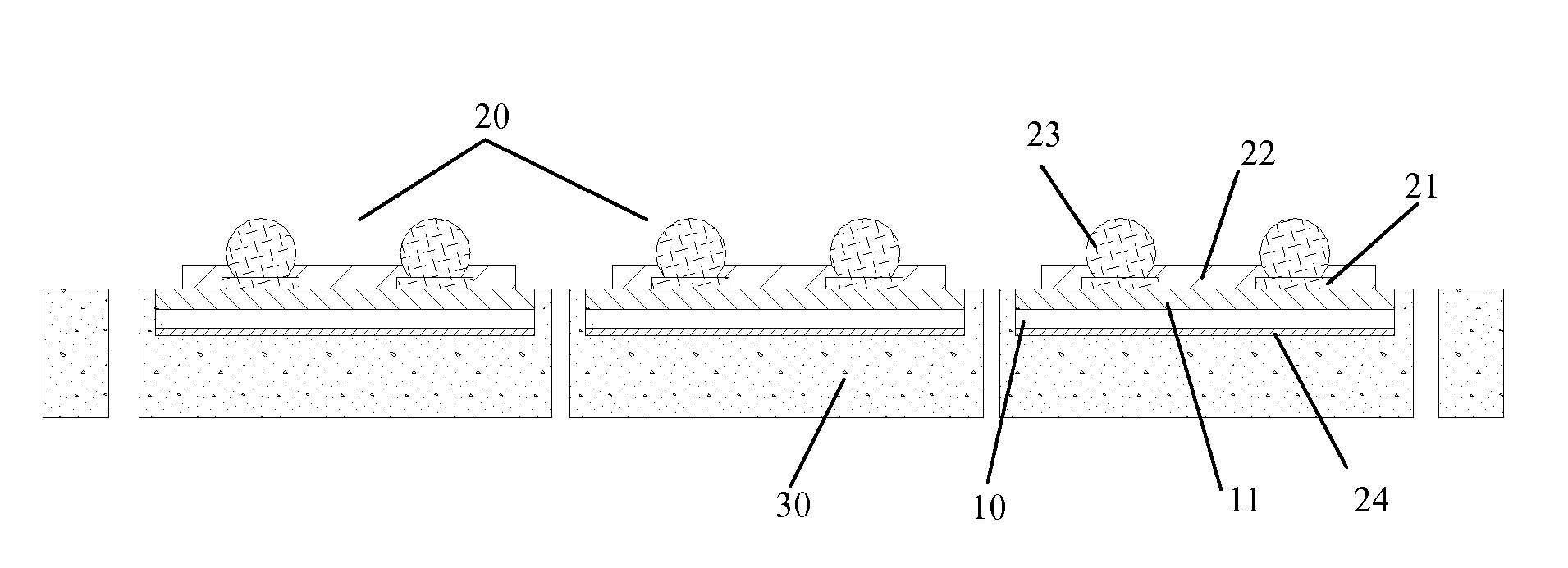
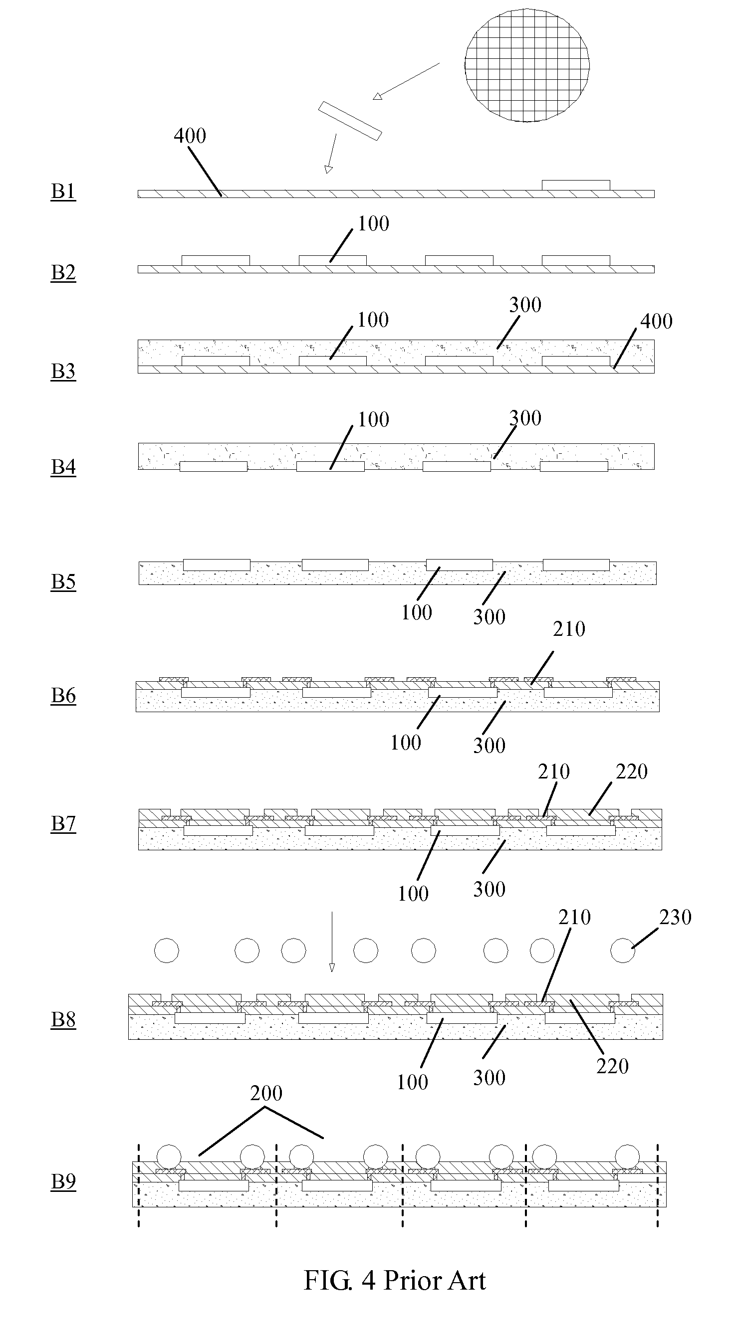
[0026]As shown in FIG. 5, the process starts with a wafer 5 including a plurality of semiconductor chips 10 formed at the front surface of the wafer 5 with the front side process for the semiconductor chips completed, in which an initial layer 11, for example a silicon oxide layer, is formed on top of the front side of the semiconductor wafer 5 and metal contact pads 21, for example aluminum pads, are formed on the initial layer 11 and electrical isolated by passivation layer 22. When the semiconductor chip package is a power device, the metal contact pads 21 can be re-distributed metal pads. Patterns for chip packages 20, shown in FIG. 14, c...


PUM


Abstract

A chip-scale packaging method, with bottom and side of a semiconductor chip encapsulated, includes the following steps: attaching backside of a thinned semiconductor wafer to a dicing tape; separating individual chips by cutting from front side of the wafer at scribe line but not cut through the dicing tape; flipping and attaching the wafer onto a top surface of a double-sided tape, then removing the dicing tape; attaching bottom surface of the double-sided tape on a supporting plate; filling the space between adjacent chips and covering the whole wafer backside with a molding material; flipping the whole structure and remove the supporting plate; placing solder balls at corresponding positions on electrodes of each chip and performing backflow treatment; finally separating individual chip packages by cutting through molding material at the space between adjacent chip packages with molding material encapsulating the bottom and side of each individual semiconductor chip.

Description

FIELD OF THE INVENTION[0001]This invention relates to a wafer level packaging (WLP) method, and particularly relates to a WLP with the side and bottom of a semiconductor chip encapsulated by a molding compound.BACKGROUND OF THE INVENTION[0002]In the advanced chip packaging methods, the WLP technique is a technique in which packaging and tests are performed on a semiconductor wafer and then the wafer is molded and singulated into individual IC packages.[0003]FIG. 1 is a cross sectional diagram of a conventional semiconductor chip package. As shown in FIG. 1, the semiconductor chip package 200 includes package body 300 surrounding the semiconductor chip 100. In addition, the semiconductor chip package 200 includes metal contact pad 210 and passivation layer 220 formed on the top surface of the semiconductor chip 100, and the solder ball 230 formed on the top electrode of the semiconductor chip 100. A packaging method of forming the semiconductor chip package 200 is shown in FIG. 2. In...

Claims


Application Information

Patent Timeline
Patent Type & Authority Patents(United States)
IPC IPC(8): H01L21/30
CPCH01L23/3114H01L23/3171H01L24/96H01L24/19H01L2924/13091H01L2224/12105H01L2924/1306H01L2924/00H01L2924/15788H01L2924/181H01L2224/02379H01L21/568H01L2924/18162
Inventor HUANG, PINGWU, RUISHENGDUAN, LEICHEN, YIGONG, YUPING
Owner ALPHA & OMEGA SEMICON INC
Why Eureka
Try Eureka