Thermally assisted dielectric charge trapping flash

a dielectric charge and flash technology, applied in the field of flash memory technology, can solve the problems of limited endurance and operation speed of charge trapping memory technology, and achieve the effects of improving endurance, improving effective endurance of the device, and improving the performance of the affected operation

Active Publication Date: 2013-07-16
MACRONIX INT CO LTD
View PDF18 Cites 19 Cited by
  • Summary
  • Abstract
  • Description
  • Claims
  • Application Information

AI Technical Summary

Benefits of technology

[0007]A memory device is described which includes resources for thermally annealing dielectric charge trapping structures of memory cells on the device. A method for operating an array of dielectric charge trapping memory cells can be applied that includes performing read, program and erase operations; and either interleaved among, or during, the read, program and erase operations, thermally annealing charge trapping structures in the memory cells in the array. Experimental results discussed below show that suitable annealing operations can improve endurance by repairing damage accumulated during program and erase cycling. For example, by periodically annealing memory cells in the array, the effective endurance of the device can be greatly improved, including achieving endurance cycling performance of 1 million cycles or more. Also, by applying the annealing during operations, such as during an erase operation, performance of the affected operation can be improved. During an erase operation for example, thermal annealing can assist electron de-trapping, and thereby improve erase speed.
[0008]Integrated circuit memory can be implemented with word line drivers and word line termination circuits, responsive to decoder circuitry and optionally other control circuits, to drive a current on corresponding word lines. The current can cause resistive heating of the selected word lines, that is transferred to the dielectric charge trapping structures for the anneal operation. This and other techniques can be applied to allow flexible delivery of the annealing operation.

Problems solved by technology

These advanced charge trapping memory technologies can have limited endurance and operation speeds, compared to other memory types.

Method used


Image

  • Thermally assisted dielectric charge trapping flash
  • Thermally assisted dielectric charge trapping flash
  • Thermally assisted dielectric charge trapping flash

Examples


Embodiment Construction

[0032]A detailed description of embodiments of the present technology is provided with reference to the FIGS. 1-21.

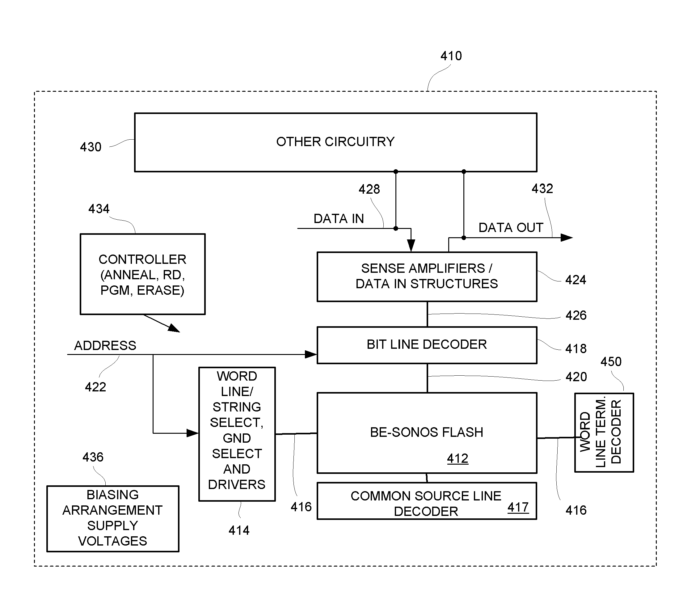
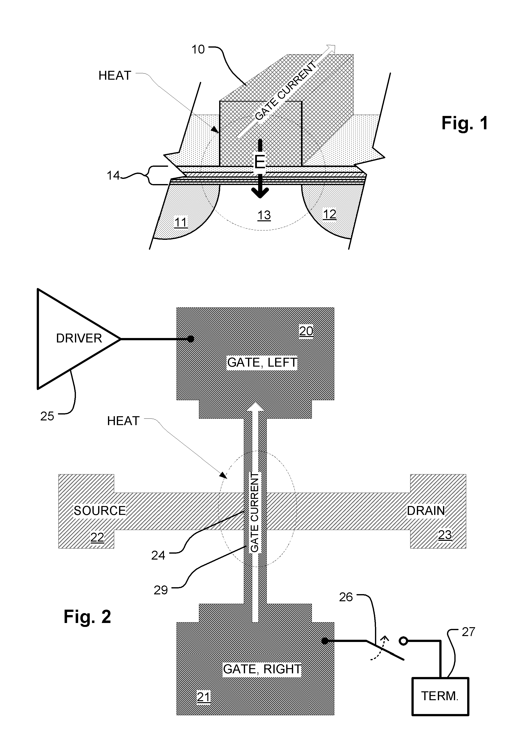
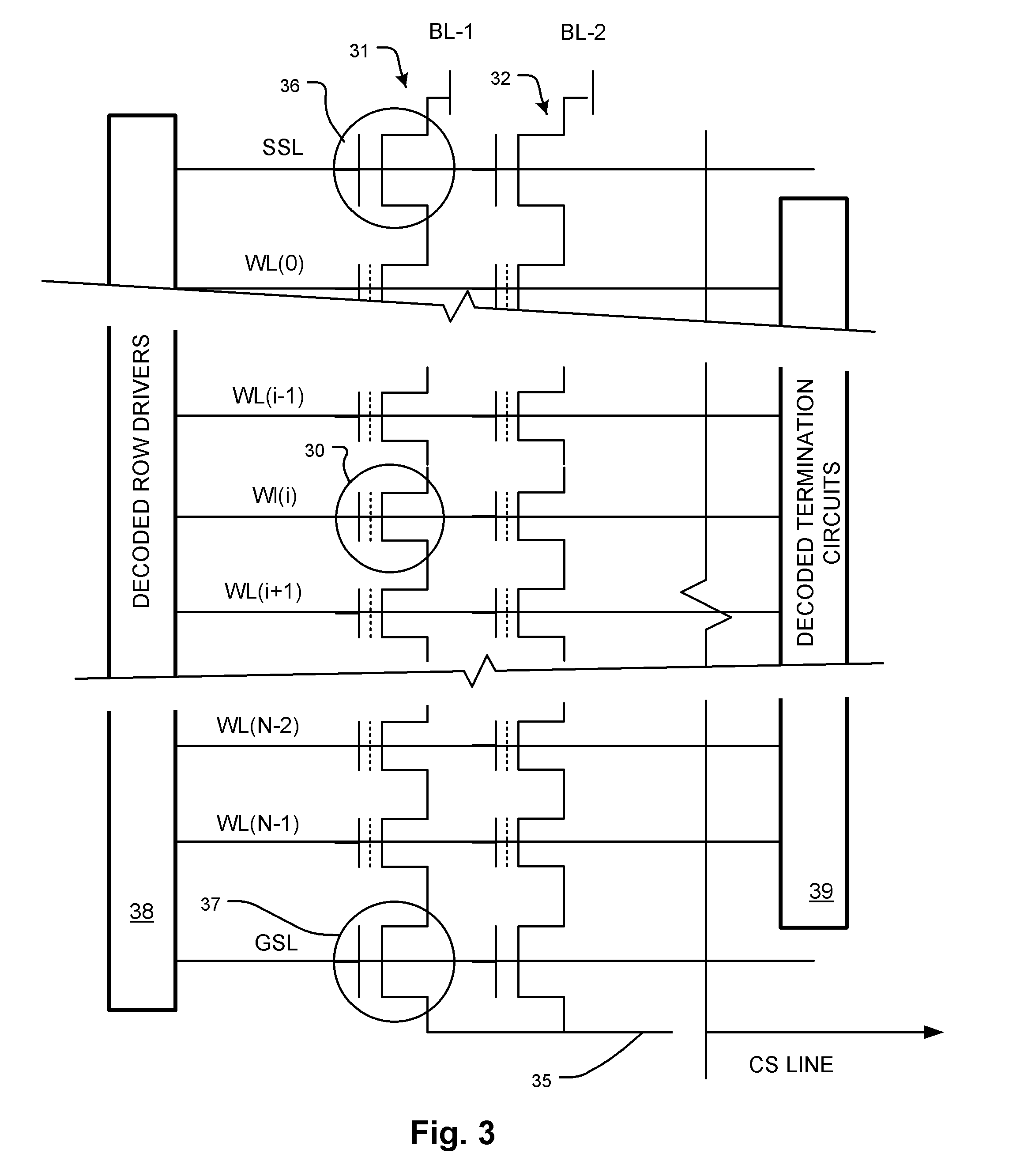
[0033]FIG. 1 is a simplified perspective view of a memory cell having a source 11 and a drain 12 in a semiconductor body 13 with a channel region between the source and drain. The word line 10 provides a gate over the channel region of the body 13. A multilayer dielectric stack 14 is interposed between gate and the channel region of the body 13, and acts as a dielectric charge trapping structure.

[0034]One technology for implementation of multilayer dielectric stack 14 is known as bandgap engineered SONOS (BE-SONOS) charge trapping technology. See, for example U.S. Pat. No. 7,315,474 by Lue, which is incorporated by reference as if fully set forth herein.

[0035]An example of a BE-SONOS multilayer dielectric stack includes a multilayer tunneling layer on the channel. The multilayer tunneling layer is implemented using a layer of silicon oxide or silicon oxynitride that is ...


PUM


Abstract

A memory device includes an array of dielectric charge trapping structures memory cells including word lines and bit lines. Control circuitry is coupled to the array arranged to control read, program and erase operations. A controller is arranged with supporting circuitry thermally annealing charge trapping structures in the memory cells in the array. Word line drivers and word line termination circuits can be used to induce current flow on the word lines to induce heat for the annealing. The thermal annealing can be applied interleaved with normal operations for recover from cycling damage. Also, the thermally annealing can be applied during mission functions like erase, to improve performance of the function.

Description

BACKGROUND OF THE INVENTION[0001]1. Field of the Invention[0002]The present invention relates to flash memory technology.[0003]2. Description of Related Art[0004]Flash memory is a class of non-volatile integrated circuit memory technology. The typical flash memory cell consists of a field effect transistor FET structure having a source and drain separated by a channel, and a gate separated from the channel by a charge storage structure including a tunnel dielectric layer, the charge storage layer (floating gate or dielectric), and a blocking dielectric layer. According to the early conventional charge trapping memory designs referred to as SONOS devices, the source, drain and channel are formed in a silicon substrate (S), the tunnel dielectric layer is formed of silicon oxide (O), the charge storage layer is formed of silicon nitride (N), the blocking dielectric layer is formed of silicon oxide (O), and the gate comprises polysilicon (S). More advanced flash memory technology has be...

Claims


Application Information

Patent Timeline
Patent Type & Authority Patents(United States)
IPC IPC(8): G11C16/04
CPCG11C16/0483G11C16/349H01L29/792G11C16/0416H10B63/80H10B63/20H01L27/0814H10B61/10
Inventor LUE, HANG-TINGCHEN, CHIH-PINGHSIEH, CHIH-CHANGHSIAO, YI-HSUAN
Owner MACRONIX INT CO LTD
Why Eureka
Try Eureka