Collapsable gate for deposited nanostructures

a nanostructure, collapsable technology, applied in the direction of transistors, electrical devices, semiconductor devices, etc., can solve the problems of reducing overly thick gate dielectric films, and affecting the quality of channel materials

Inactive Publication Date: 2013-07-23
GLOBALFOUNDRIES INC
View PDF16 Cites 10 Cited by
  • Summary
  • Abstract
  • Description
  • Claims
  • Application Information

AI Technical Summary

Problems solved by technology

However, the relative inertness of the channel material (lack of dangling bonds or chemically active sites) means that most gate dielectric materials and deposition techniques do not wet the surface of the nanostructure well.
This approach results in overly thick gate dielectric films, however, because the nucleation on the graphene layer or the CNT proceeds in an island growth mode.
Similarly, the surface of the graphene layer or the CNT may be slightly damaged through physical bombardment or plasma processes to create dangling bonds.
However, this functionalization process reduces the quality of the channel material, reducing charge mobility and overall performance of the resulting FET.
However, very thin films less than 10 nm in thickness are difficult to obtain with spin-on materials, and spin-on gate dielectrics tend to be of relatively low quality and contain a lot of trapped charges and impurities, resulting in devices with large hysteresis, poor subthreshold slope and poor repeatability.
In addition, graphene layers and carbon nanotubes are vulnerable to degradation from exposure to energetic oxygen species or plasma processes.
Unfortunately, a large number of semiconductor processes, including plasma enhanced chemical vapor deposition (PECVD), reactive ion etching (RIE), and deposition of oxides by chemical vapor deposition (CVD) or physical vapor deposition (PVD), involve either energetic oxygen species or plasma processes.
This greatly limits the number of microfabrication techniques that can be leveraged for the fabrication of graphene-based devices and CNT-based devices.

Method used


Image

  • Collapsable gate for deposited nanostructures
  • Collapsable gate for deposited nanostructures
  • Collapsable gate for deposited nanostructures

Examples


Embodiment Construction

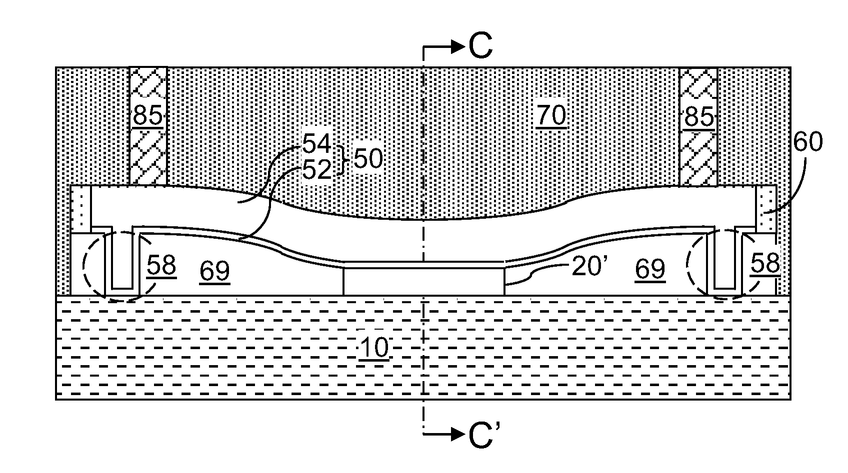
[0034]As stated above, the present disclosure relates to devices including at least one 2-dimensional carbon lattice structure, and particularly to field effect transistors including at least one 2-dimensional carbon lattice structure, and methods of manufacturing the same, which are now described in detail with accompanying figures. Like and corresponding elements mentioned herein and illustrated in the drawings are referred to by like reference numerals. The drawings are not necessarily drawn to scale.

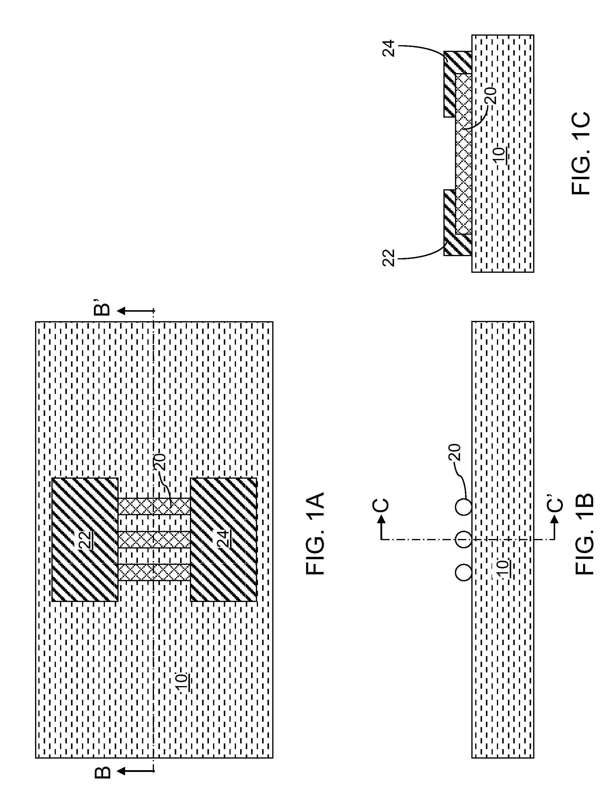
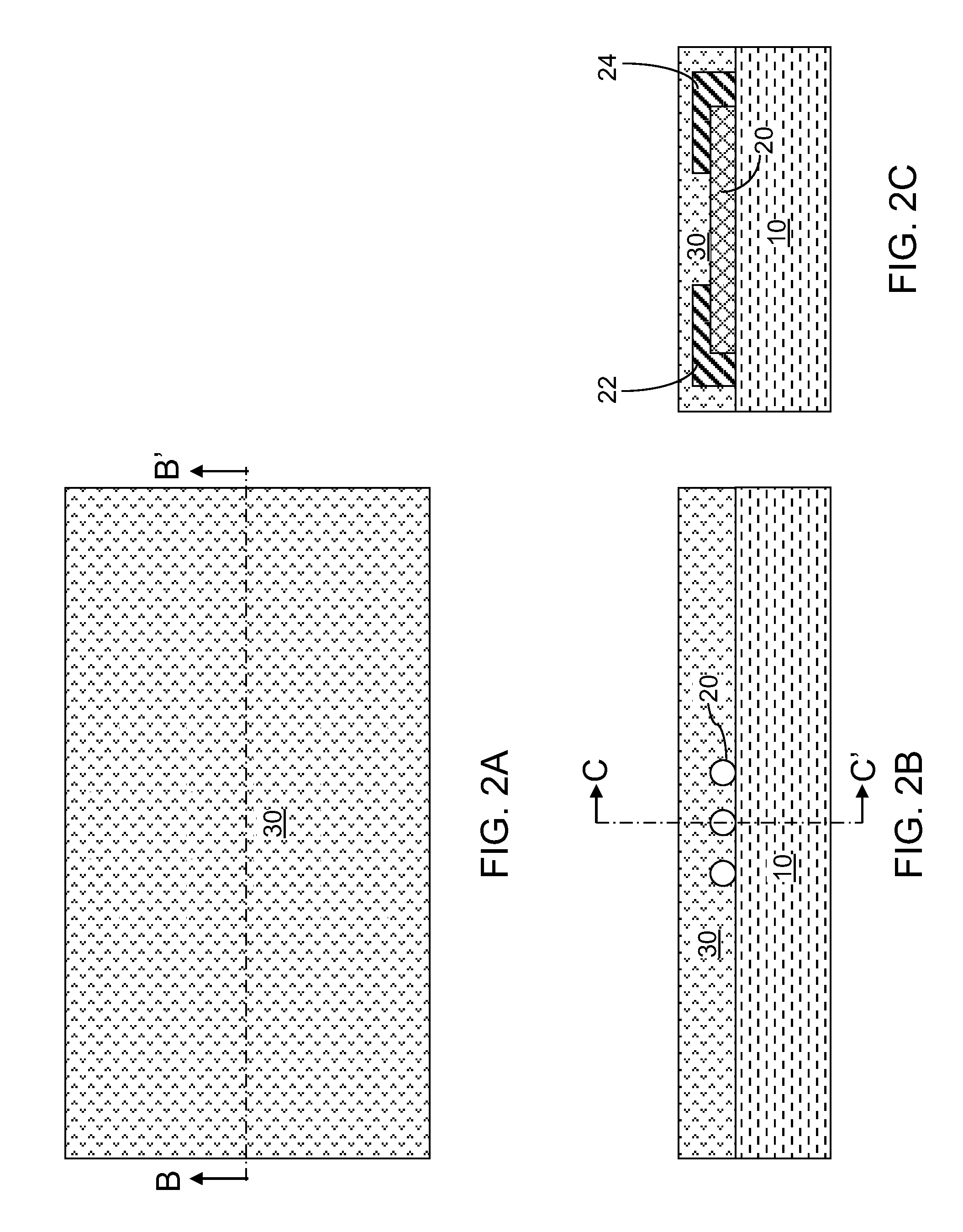
[0035]Referring to FIGS. 1A-1C, a first exemplary structure according to a first embodiment of the present disclosure includes an insulator layer 10, which can be a substrate that stands alone or can be an upper portion of a substrate including another substrate portion (not shown) located underneath the insulator layer 10. The insulator layer 10 can be, for example, a silicon oxide layer, a silicon nitride layer, an aluminum oxide layer, or any other dielectric material layer.

[0036]...


PUM

PropertyMeasurementUnit
thicknessaaaaaaaaaa
diametersaaaaaaaaaa
thicknessesaaaaaaaaaa

Abstract

A disposable material layer is first deposited on a graphene layer or a carbon nanotube (CNT). The disposable material layer includes a material that is less inert than graphene or CNT so that a contiguous dielectric material layer can be deposited at a target dielectric thickness without pinholes therein. A gate stack is formed by patterning the contiguous dielectric material layer and a gate conductor layer deposited thereupon. The disposable material layer shields and protects the graphene layer or the CNT during formation of the gate stack. The disposable material layer is then removed by a selective etch, releasing a free-standing gate structure. The free-standing gate structure is collapsed onto the graphene layer or the CNT below at the end of the selective etch so that the bottom surface of the contiguous dielectric material layer contacts an upper surface of the graphene layer or the CNT.

Description

BACKGROUND[0001]The present disclosure generally relates to devices including at least one 2-dimensional carbon lattice structure, and particularly to field effect transistors including at least one 2-dimensional carbon lattice structure, and methods of manufacturing the same.[0002]The ability to deposit a thin, pinhole-free gate dielectric on carbon nanostructures such as graphene and carbon nanotubes (CNTs) is important to enable the fabrication of field effect transistors with good electrostatics. However, the relative inertness of the channel material (lack of dangling bonds or chemically active sites) means that most gate dielectric materials and deposition techniques do not wet the surface of the nanostructure well.[0003]In a first approach, a sufficient amount of dielectric material may be deposited until a surface of a graphene layer or a CNT is coated with a contiguous layer of the dielectric material. This approach results in overly thick gate dielectric films, however, be...

Claims


Application Information

Patent Timeline
Patent Type & Authority Patents(United States)
IPC IPC(8): H01L29/06H01L51/40H01L29/15H01L31/00
CPCH01L29/66045H01L51/055H10K10/481
Inventor CHANG, JOSEPHINE B.CHANG, PAULGUILLORN, MICHAEL A.WAGGONER, PHILIP S.
Owner GLOBALFOUNDRIES INC
Why Eureka
Try Eureka