Direct DC coupled push-pull BJT driver for power amplifier with built-in gain and bias current signal dependent expansion

a power amplifier and push-pull technology, applied in the direction of amplifiers, amplifiers with semiconductor devices/discharge tubes, amplifiers, etc., can solve the problems of large output impedance transformation ratios, and significant losses in power combining circuits, etc., to achieve maximum output power, high voltage handling capability, and high ruggedness

Active Publication Date: 2013-07-30
SKYWORKS SOLUTIONS INC
View PDF1 Cites 17 Cited by
  • Summary
  • Abstract
  • Description
  • Claims
  • Application Information

AI Technical Summary

Benefits of technology

[0015]The present invention proposes an improved driver circuit for driving a Radio Frequency or Microwave power amplifier with built-in gain and bias current signal dependent expansion in order to obtain a maximum output power through a linearized power amplifier. In an embodiment, the driver circuit includes an output stage made of GaAs or GaN material which is integrated with a programmable driver stage having high voltage handling capability in order to attain high ruggedness and maximum output power through linearized transfer characteristics of the power amplifier.
[0016]An embodiment of the present invention, minimizes the amount of costly compound semiconductor material with low cost silicon material (in this case CMOS) while realizing only a final stage amplifier in a high power capable GaAs process within a single module. A silicon driver, realized in a CMOS process, enables flexibility provided by a digital programmability readily available in modern silicon processes. This enables optimization and enhancement of amplifier performance. A CMOS driver architecture also minimizes the size of the costly high power stage by eliminating the need for area consuming inter-stage matching components and bias circuitry by providing both DC and RF drive simultaneously.
[0017]Normally, the Radio Frequency hereinafter referred to as “RF” and Microwave amplifiers using a Bipolar and a Heterojunction Bipolar Transistor (HBT) are biased in an AB class mode. In this case, a diode of a reference biasing transistor is directly exposed to an RF input signal which creates a self biasing effect where a bias current increases with an increasing input power level. This, in turn, linearizes the transfer characteristics of the power amplifier, but makes the design very sensitive to parameter values chosen in a bias circuit and also engenders strange and undesirable frequency characteristics. The effects mentioned above are very hard to simulate and hence the design process becomes experimental and iterative which results in very long design cycles. Therefore, it makes the design very technology dependent and process transfers very complicated and expensive.

Problems solved by technology

On the other hand, the active field of CMOS power amplifier design needs much effort directed towards the creation of the needed output power using power combiners.
However, the low voltage handling capability of normal CMOS transistors forces the usage of very large output impedance transformation ratios, which in turn end up encountering significant losses in the power combining circuit.
Therefore, the performance of the power amplifier in terms of maximum output power, power added efficiency and ruggedness is therefore compromised relative to a GaAs based power amplifier.

Method used


Image

  • Direct DC coupled push-pull BJT driver for power amplifier with built-in gain and bias current signal dependent expansion
  • Direct DC coupled push-pull BJT driver for power amplifier with built-in gain and bias current signal dependent expansion
  • Direct DC coupled push-pull BJT driver for power amplifier with built-in gain and bias current signal dependent expansion

Examples


Embodiment Construction

[0026]The detailed description of the appended drawings is intended as a description of the currently preferred embodiments of the present invention, and is not intended to represent the only form in which the present invention may be practiced. It is to be understood that the same or equivalent functions may be accomplished by different embodiments that are intended to be encompassed within the spirit and scope of the present invention.

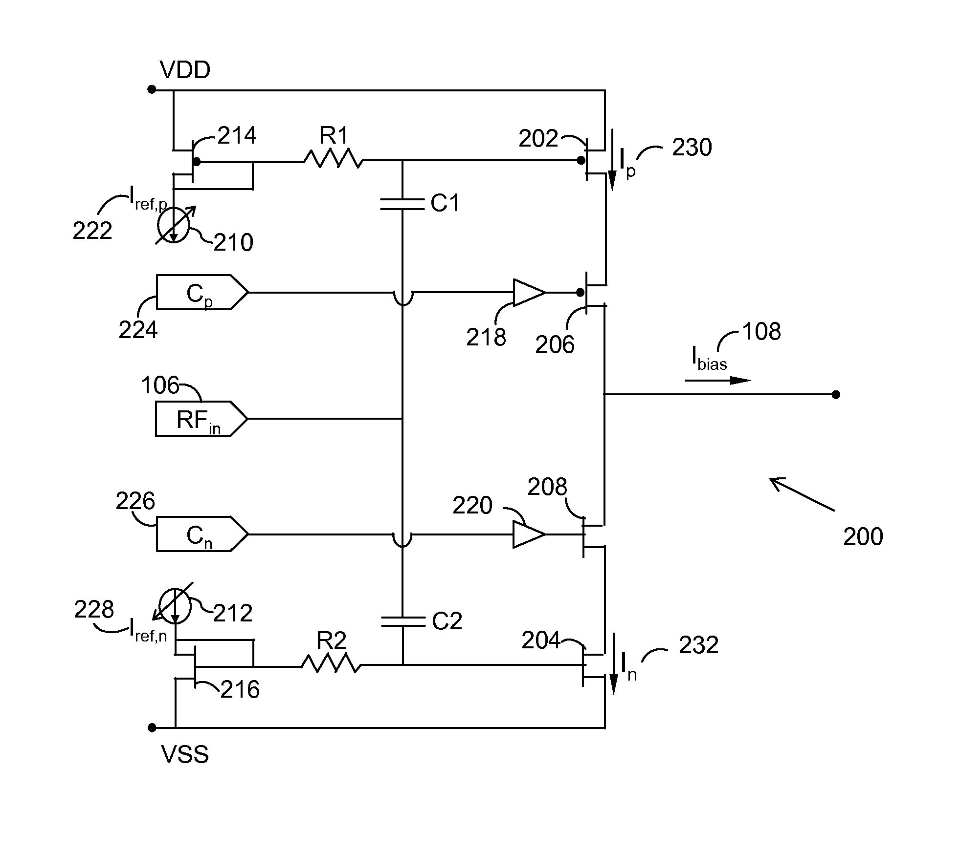
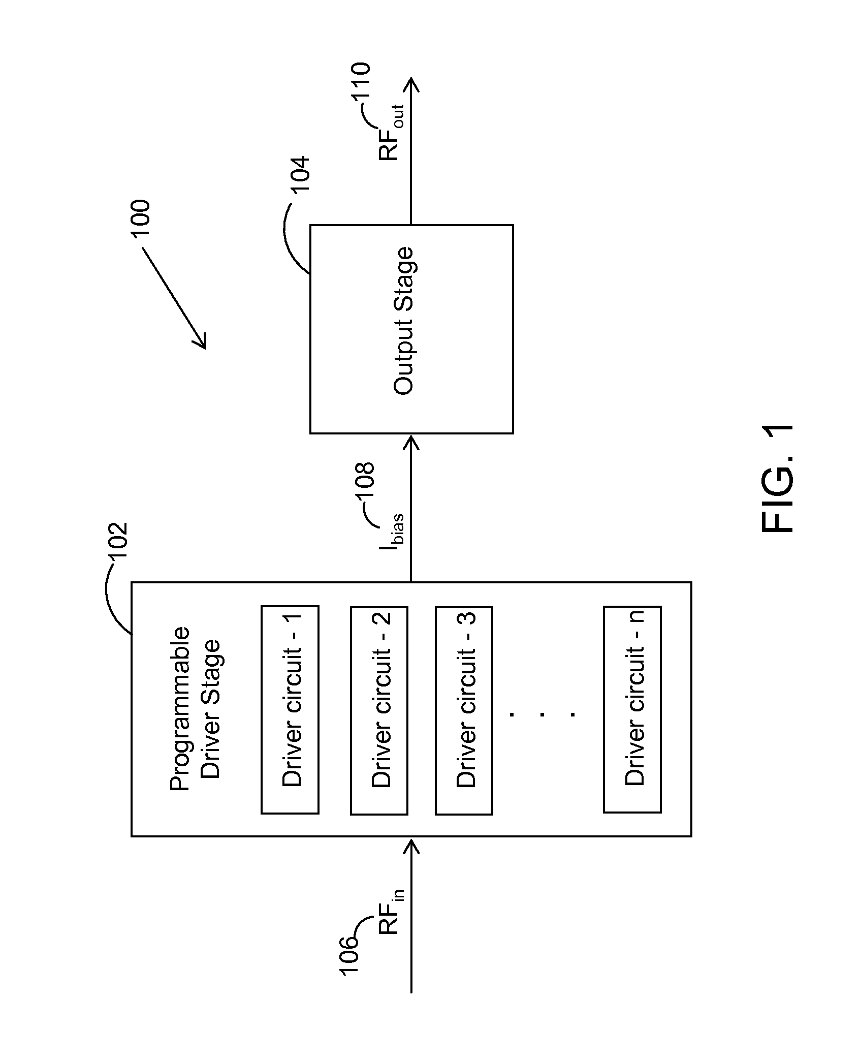
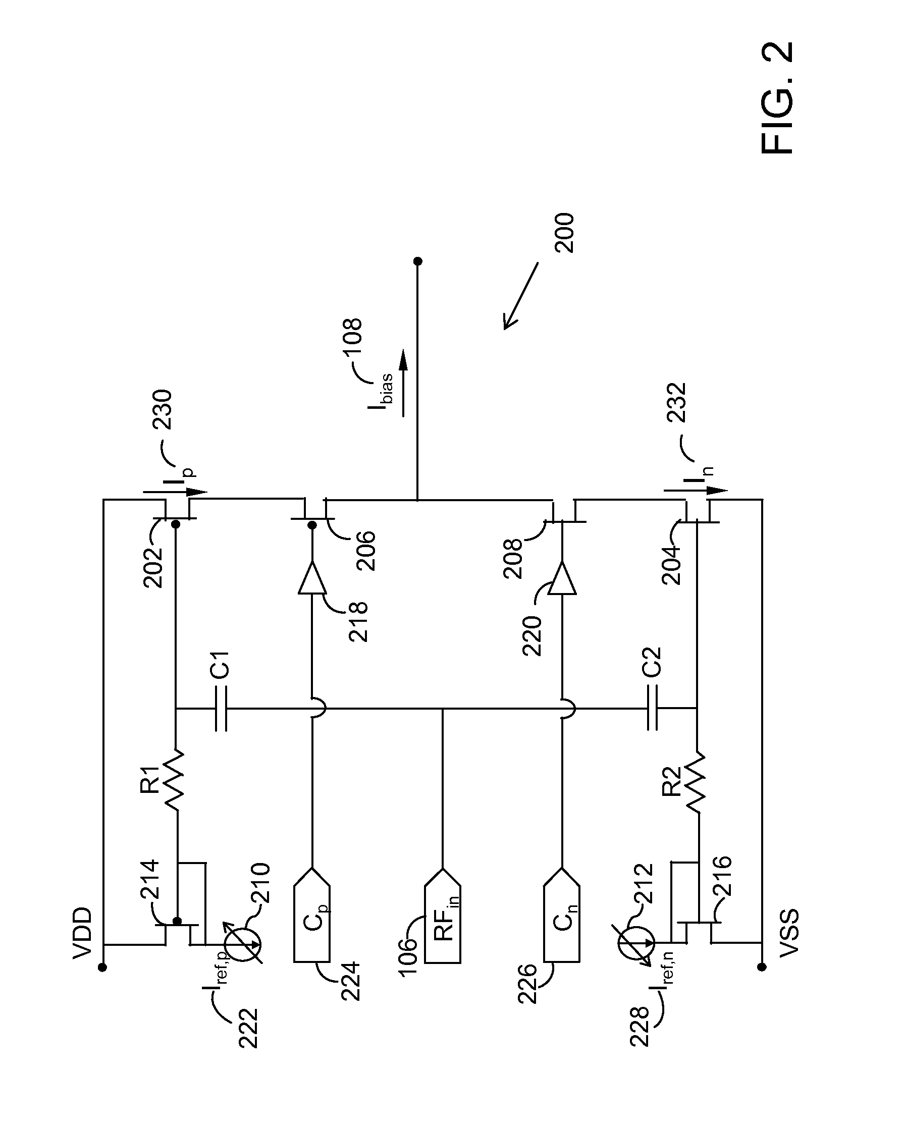
[0027]The present invention proposes an improved driver circuit for driving a Radio Frequency or Microwave power amplifier with built-in gain and bias current signal dependent expansion in order to obtain a maximum output power through a linearized power amplifier. In an embodiment, the driver circuit includes an output stage made of GaAs or GaN material which is integrated with a programmable driver stage having high voltage handling capability in order to attain high ruggedness and maximum output power through linearized transfer characteristics of...


PUM


Abstract

A power amplifier having a driver stage and an output stage is configured to provide an amplified RF input signal. The driver stage of the power amplifier consists of one or more driver circuits consisting of a network of transistors, current sources, capacitive elements and resistive elements. An RF input signal is fed into the driver stage which is configured to provide a dynamic DC bias and an RF signal gain to a base terminal of a Bipolar Junction Transistor (BJT) power device present in the output stage. The output stage includes of a network of transistors, capacitive and resistive elements and when driven by the DC bias and the RF signal from the driver stage produces an amplified RF input signal at an output side of the output stage.

Description

CROSS REFERENCE TO RELATED APPLICATIONS[0001]This application claims priority from U.S. provisional application Ser. No. 61 / 408,855 filed Nov. 1, 2010, the disclosure of which is hereby incorporated by reference.TECHNICAL FIELD[0002]The present invention relates, in general, to power amplifiers. More specifically, the present invention relates to the driver circuits used in Radio Frequency (RF) and Microwave power amplifiers in the field of cellular communication.BACKGROUND[0003]Cellular communication systems have entered our daily life since the early nineties. Recent years have seen tremendous improvements in the field of cellular communication which has led to an unprecedented wireless revolution. The main reason for these improvements is the achievable high integration level of Complementary Metal Oxide Semiconductors (CMOS), hereinafter referred to as CMOS. This gave rise to the integration of a huge number of digital functionalities into a single chip which resulted in the pow...

Claims


Application Information

Patent Timeline
Patent Type & Authority Patents(United States)
IPC IPC(8): H03F3/26
CPCH03F3/19H03F3/3022
Inventor LEIPOLD, DIRKALLEN, WADEHAU, GARY
Owner SKYWORKS SOLUTIONS INC
Why Eureka
Try Eureka