Solid-state image pickup device, image pickup apparatus including the same, and method of manufacturing the same

a pickup device and solid-state technology, applied in the direction of transistors, television systems, radio control devices, etc., can solve the problems of remarkable reduction in light receiving efficiency due to the reduction of the area of the photodiode, and achieve the effect of enhancing function

Active Publication Date: 2013-08-27
SONY CORP
View PDF1 Cites 8 Cited by
  • Summary
  • Abstract
  • Description
  • Claims
  • Application Information

AI Technical Summary

Benefits of technology

[0009]As a result, in the pixel circuit disposed in the solid-state image pickup device disclosed in Patent Document 1, an area of the photodiode in the light receiving area of the semiconductor substrate becomes small. When the area of the photodiode becomes small, a light receiving efficiency of the photodiode is reduced.
[0011]The present invention has been made in order to solve the problems described above, and it is therefore desirable to provide a solid-state image pickup device in which functionality is enhanced while reduction in an area of a photoelectric conversion element such as a photodiode is suppressed to the minimum, an image pickup apparatus including the same, and a method of manufacturing the same.
[0016]According to the present invention, the functionality can be enhanced while the reduction of the photoelectric conversion element such as the photodiode is suppressed to the minimum.

Problems solved by technology

Also, in the pixel circuit disposed in the solid-state image pickup device disclosed in Patent Document 1, when a pitch of the photodiodes in a plurality of pixel circuits is set as the order of 1 micrometer or less (or the order of 2 micrometers or less), there is the possibility that a problem of reduction in the light receiving efficiency due to the reduction in the area of the photodiode is remarkably caused.

Method used


Image

  • Solid-state image pickup device, image pickup apparatus including the same, and method of manufacturing the same
  • Solid-state image pickup device, image pickup apparatus including the same, and method of manufacturing the same
  • Solid-state image pickup device, image pickup apparatus including the same, and method of manufacturing the same

Examples


first embodiment

1. First Embodiment

Configuration of CMOS Image Sensor

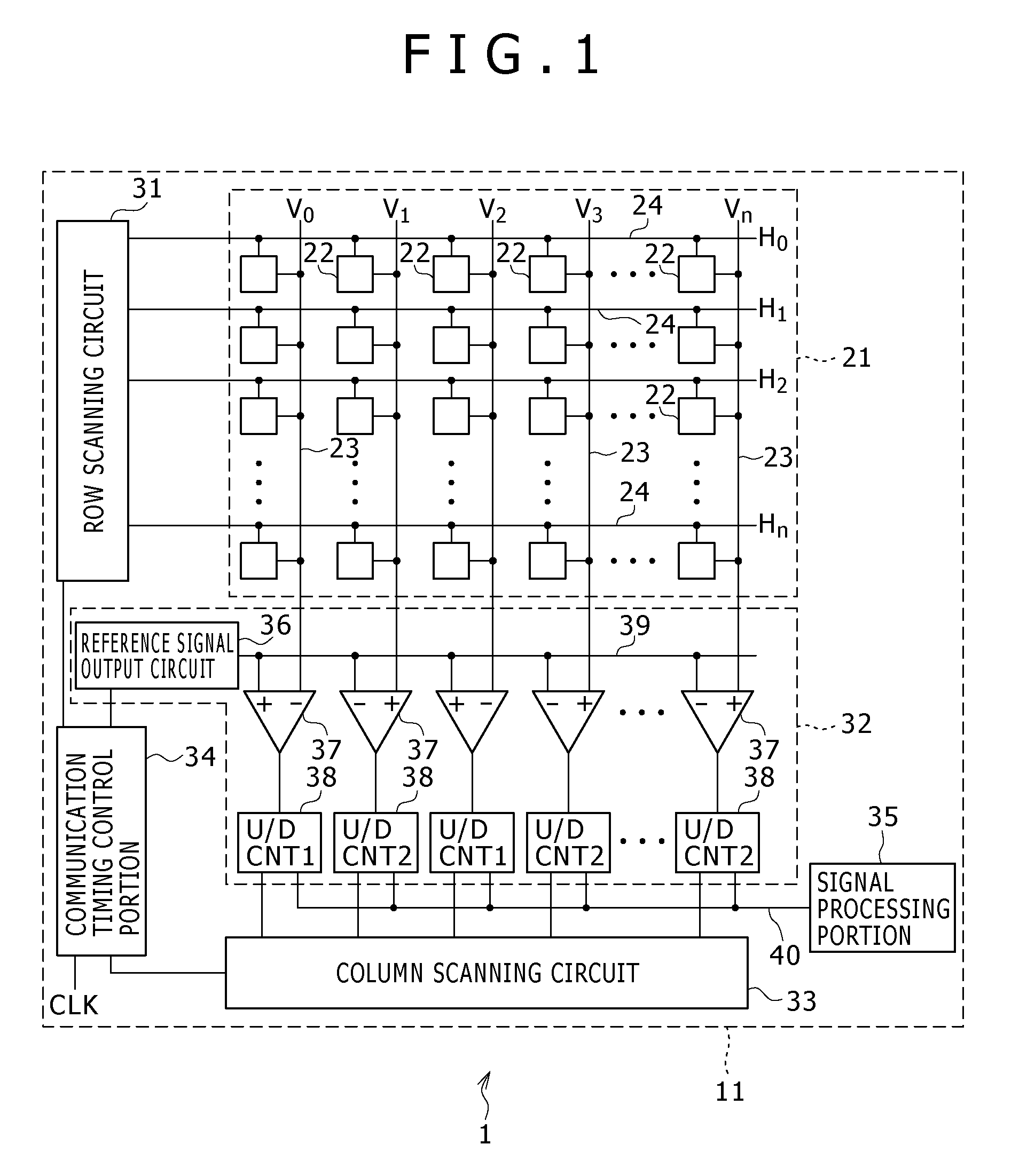
[0033]FIG. 1 shows a schematic layout of a Complementary Metal Oxide Semiconductor (CMOS) image sensor 1 utilizing a column Analog-to-Digital (A / D) conversion system to which a solid-state image pickup device according to a first embodiment of the present invention is applied.

[0034]The CMOS image sensor 1 has a semiconductor substrate 11.

[0035]A light receiving area 21 is set in the semiconductor substrate 11.

[0036]The light receiving area 21 is a rectangular area in which an aspect ratio, for example, is set as either 3:4 or 9:16.

[0037]Also, a plurality of pixel circuits 22 are formed in the light receiving area 21.

[0038]A plurality of pixel circuits 22 are two-dimensionally disposed in a matrix in the light receiving area 21.

[0039]In addition, a plurality of column signal lines (read signal lines) 23, and a plurality of row signals 24 are wired in the light receiving area 21. In this case, the number of column signal lines 23 is...

second embodiment

2. Second Embodiment

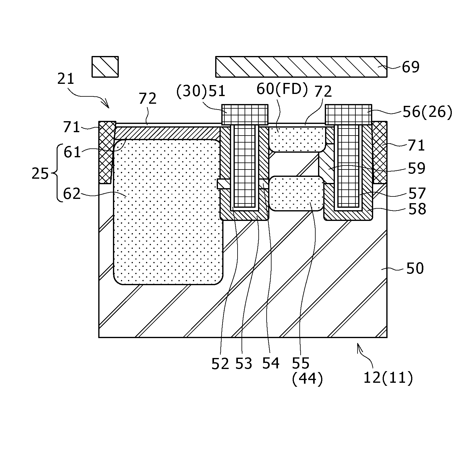
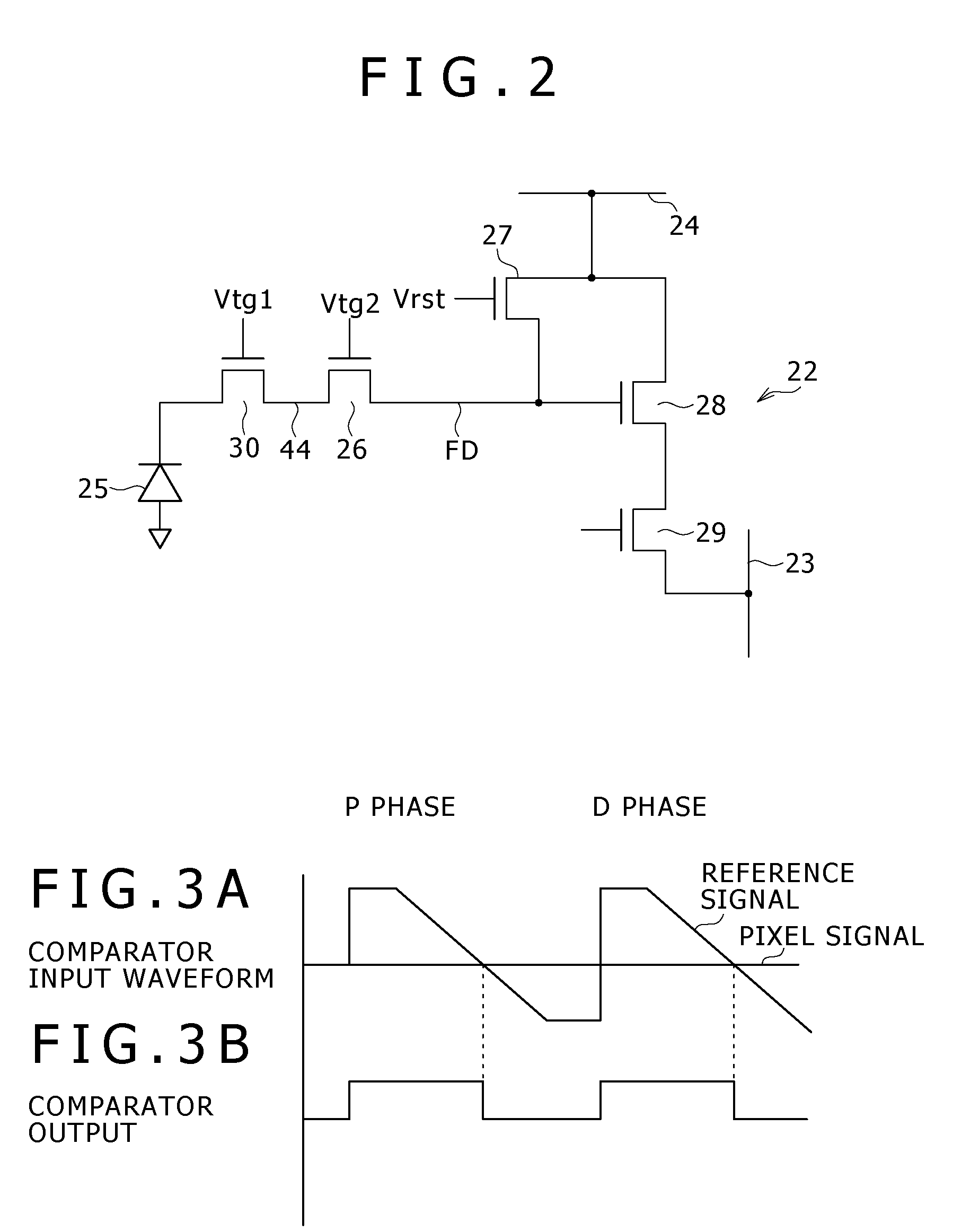
[0286]A CMOS image sensor 1 according to a second embodiment of the present invention is such that one floating diffusion FD is formed for a plurality of pixel circuits 22.

[0287]FIG. 10 is a top plan view showing a schematic layout of four pixel circuits 22 formed on the semiconductor substrate 11 in the CMOS image sensor 1 according to the second embodiment of the present invention.

[0288]The four (=2(row)×2(column)) pixel circuits 22 are shown in FIG. 10.

[0289]Also, as shown in FIG. 10, a plurality of pixel circuits 22 are formed on the semiconductor substrate 11 in the second embodiment based on a repetitive pattern for each four (=2(row)×2(column)) pixel circuits 22.

[0290]Specifically, a top-left pixel circuit 22-1 including a photodiode 25-1, a first transfer transistor 30-1, and a second transfer transistor 26-1 is formed in a top-left pixel circuit formation area shown in FIG. 10.

[0291]In addition, a bottom-left pixel circuit 22-2 including a photodiode 25-...

third embodiment

3. Third Embodiment

Configuration of Image Pickup Apparatus

[0314]FIG. 12 shows a schematic configuration of a camera system 101 to which an image pickup apparatus according to a third embodiment of the present invention is applied.

[0315]The camera system 101 is either a digital still camera or a digital video camera to which the CMOS image sensor (solid-state image pickup device) 1 of any of the first and second embodiment described above is mounted.

[0316]It is noted that the camera system 101 may be incorporated as a camera module or the like in a mobile apparatus such as a mobile phone.

[0317]The camera system 101 shown in FIG. 12 includes a lens group 102 composing an optical system, the CMOS image sensor 1, a Digital Signal Processor (DSP) circuit 103, a display device 104, a manipulation system device 105, a frame memory 106, a recording device 107, and a power source system device 108.

[0318]The DSP circuit 103 is connected to the CMOS image sensor 1. The DSP circuit 103 processe...


PUM


Abstract

A solid-state image pickup device in which electric charges accumulated in a photodiode conversion element are transferred to a second diffusion layer through a first diffusion layer.

Description

BACKGROUND OF THE INVENTION[0001]1. Field of the Invention[0002]The present invention relates to a solid-state image pickup device in which a plurality of photoelectric conversion elements are disposed on a semiconductor substrate, an image pickup apparatus including the same, and a method of manufacturing the same.[0003]2. Description of the Related Art[0004]Japanese Patent Laid-Open No. 2006-311515 (hereinafter referred to as Patent Document 1) discloses a solid-state image pickup device having a plurality of pixel circuits.[0005]In each of the pixel circuits disposed in the solid-state image pickup device disclosed in Patent Document 1, a first transfer gate, a first floating diffusion layer, a second transfer gate, and a second floating diffusion layer are connected to a photodiode in this order.[0006]Also, in each of the pixel circuits disposed in the solid-state image pickup device disclosed in Patent Document 1, the electric charges accumulated in the photodiode are supplied ...

Claims


Application Information

Patent Timeline
Patent Type & Authority Patents(United States)
IPC IPC(8): H01L31/062H01L31/113H01L27/146H04N5/335H04N5/369H04N5/374
CPCH01L27/14609H01L27/14612H01L27/14689H01L27/14643
Inventor MASAGAKI, ATSUSHIYAMAMURA, IKUHIRO
Owner SONY CORP
Why Eureka
Try Eureka