Nonvolatile memory cell comprising a nanowire and manufacturing method thereof

a memory cell and nanowire technology, applied in the field of memory cells, can solve the problems of low coupling ratio, high operating voltage, and inability to properly scale standard planar flash memory beyond 50 nm, and achieve the effects of reducing the number of word lines, and avoiding or suppressing artefacts

Active Publication Date: 2013-10-01
MARLIN SEMICON LTD
View PDF12 Cites 11 Cited by
  • Summary
  • Abstract
  • Description
  • Claims
  • Application Information

AI Technical Summary

Benefits of technology

[0029]According to an exemplary embodiment of the invention, a method of producing memory cells is provided in which vertical nanowires are grown or are formed using an etching procedure as channels of transistors of the memory cells, wherein a gate stack may be partially or all-wrapped around the respective channel, for instance to form a coaxial structure. Furthermore, the nanowires may be grown within trenches surrounded by electrically insulating structures such as silicon oxide that provides electrical isolation between word lines in a memory array configuration. By taking this measure, it may be made possible to improve scaling issues. In other words, an area required for a memory array may be scaled down to a great extent with enhanced control over the channel. Beyond this, efficient process integration is possible to build memory arrays with vertical nanowire-based transistors.
[0062]In an embodiment of the invention in which a floating gate configuration is implemented, programming a memory cell may be performed by applying a voltage of 12 V to 15 V to the control gate, and by simultaneously grounding the two source / drain regions (i.e. source and drain). Then, charge carriers may be injected into the floating gate by Fowler-Nordheim tunnelling. Since embodiments of the invention significantly improve the coupling efficiency, the programming voltage may be reduced compared to conventional approaches. Reading out a memory cell may be performed by applying a voltage of 1 V to the control gate, by applying a voltage of 0.5 V to the drain and by grounding the source. A voltage of 1 V may be applied to the access gate. Erasing a memory cell may be performed by applying a voltage of −12 V to −15 V to the control gate, and by simultaneously grounding the two source / drain regions (i.e. source and drain), so that charge carriers may be injected into or removed from the floating gate by Fowler-Nordheim tunnelling. The given voltage values are only examples and may vary over a broad interval. They may depend on dimensions, materials and electronic characteristics of the memory cell such as the threshold voltage of the transistor(s).

Problems solved by technology

However, it is a problem that a standard planar flash memory cannot be scaled properly beyond 50 nm.
Particularly, the scaling of tunnel and control dielectric thickness is limited by concerns for data-retention, yielding low coupling ratios and consequently high operating voltages.
These circumstances result in the fact that future scaled cells suffer of short channel effects and punch through phenomena, as well as of small on-current / off-current ratio, thus reducing the sensing margin.
However, double gate and FinFET transistors are difficult in manufacture and operation.
However, with the procedure of forming a memory arrangement according to US 2003 / 0015755 A1, it may be difficult to obtain a sufficient integration density of memory cells.
Furthermore, the manufacturing procedure according to US 2003 / 0015755 A1 is difficult and cost intensive.

Method used


Image

  • Nonvolatile memory cell comprising a nanowire and manufacturing method thereof
  • Nonvolatile memory cell comprising a nanowire and manufacturing method thereof
  • Nonvolatile memory cell comprising a nanowire and manufacturing method thereof

Examples


Embodiment Construction

[0078]The illustration in the drawing is schematical. In different drawings, similar or identical elements are provided with the same reference signs.

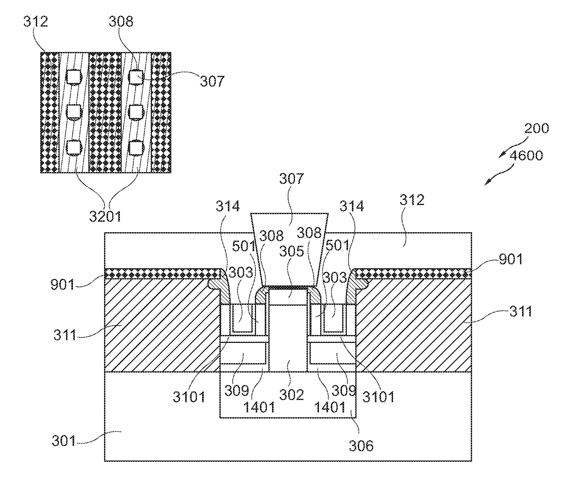
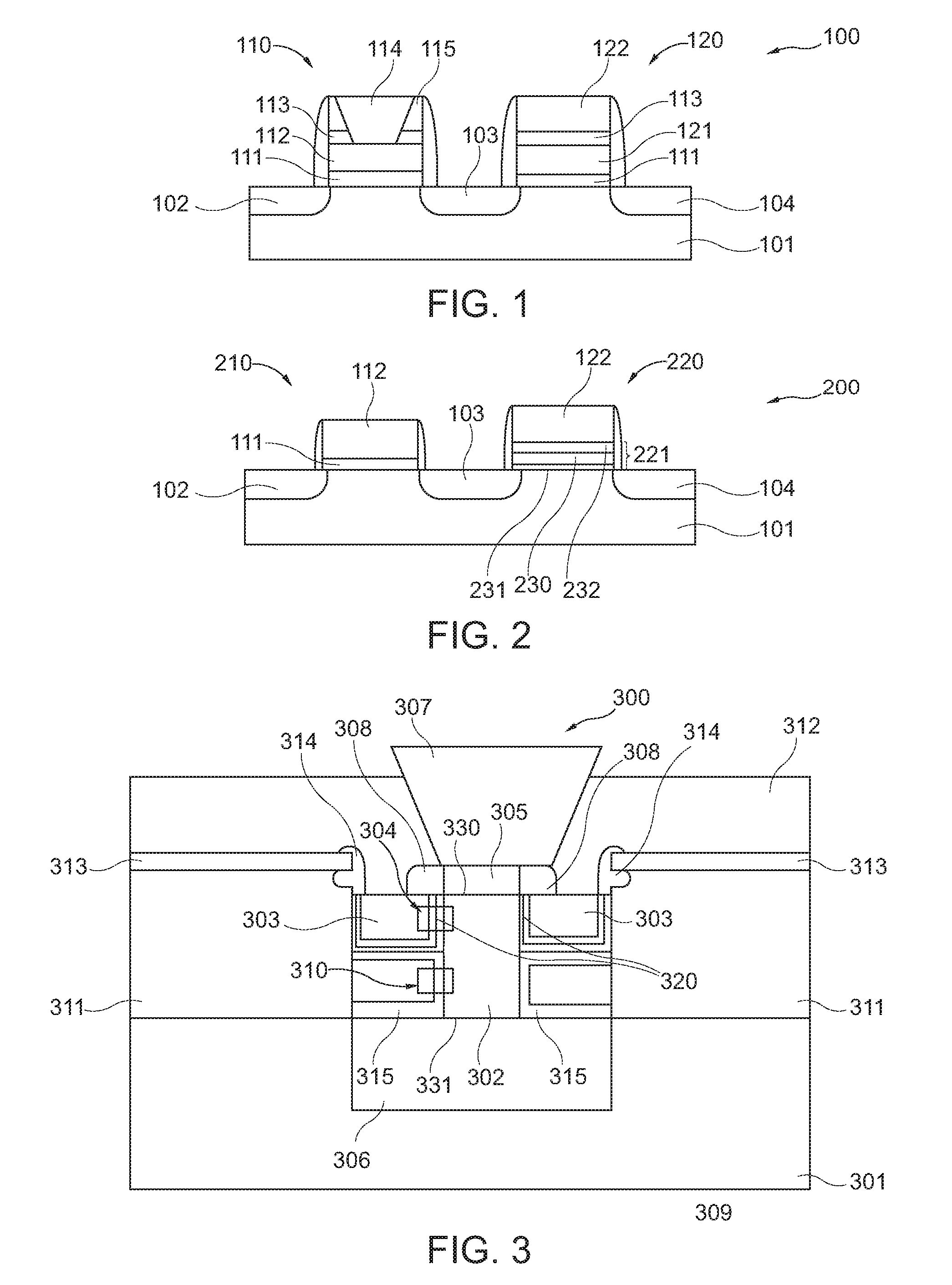
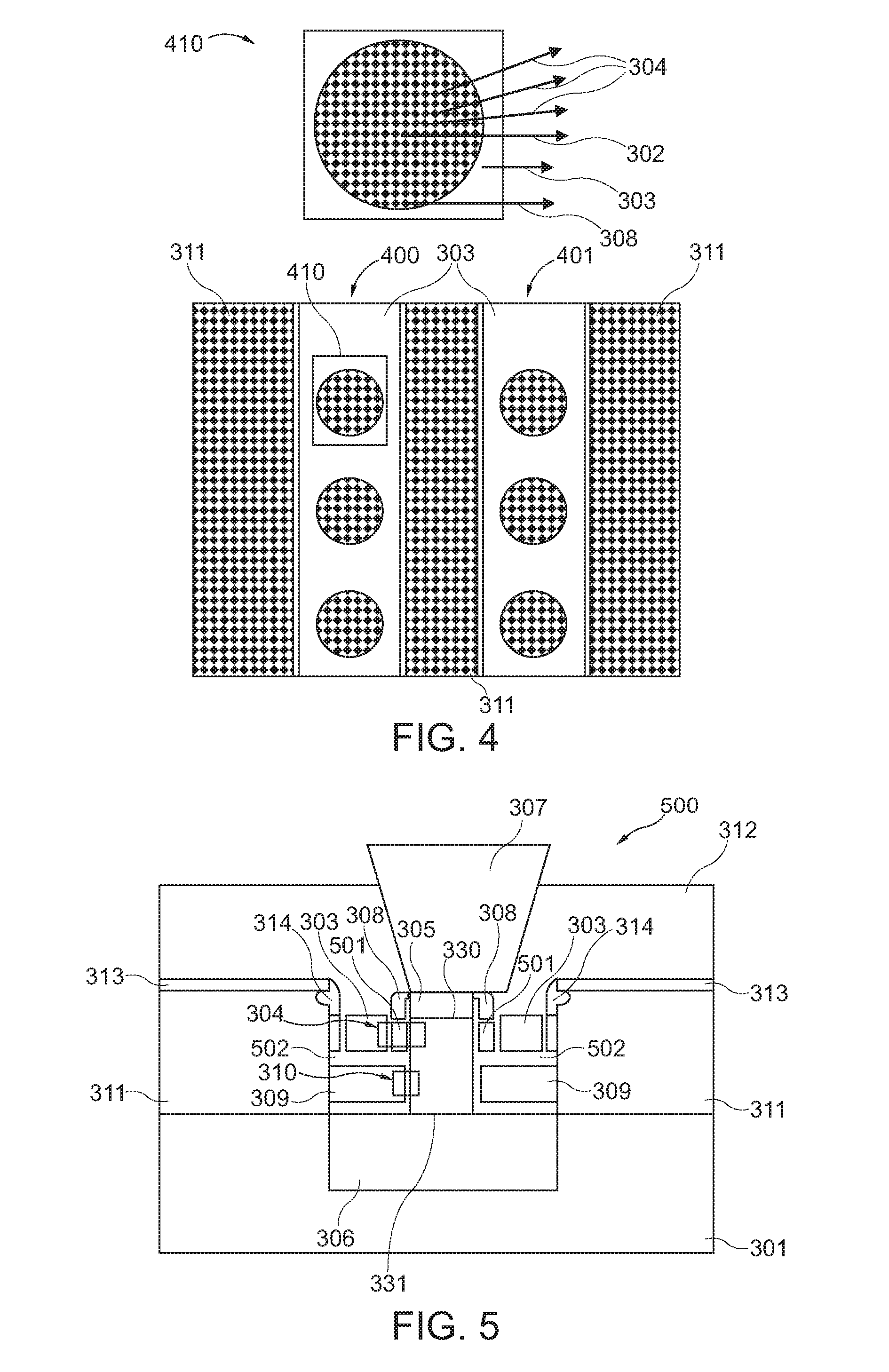
[0079]In the following, referring to FIG. 3, a memory cell 300 according to an exemplary embodiment of the invention will be explained.

[0080]The memory cell 300 comprises a substrate 301 that is an n-type silicon wafer. An oblong nanowire 302 extends along a vertical trench formed in the substrate 301. Furthermore, a control gate 303 is provided which surrounds the nanowire 302 in a coaxial manner along a portion of the vertical extension of the nanowire 302. A charge storage structure 304 is formed as an ONO layer sequence and is arranged between the control gate 303 and the nanowire 302. Actually, the charge will be stored in the nitride layer of the ONO layer sequence 304.

[0081]The memory cell 300 further comprises a first source / drain region 305 (which may particularly act as a drain) and is formed by an n+-doped silicon material. ...


PUM


Abstract

A memory cell, the memory cell comprising a substrate, a nanowire extending along a vertical trench formed in the substrate, a control gate surrounding the nanowire, and a charge storage structure formed between the control gate and the nanowire.

Description

FIELD OF THE INVENTION[0001]The invention relates to a memory cell.[0002]Moreover, the invention relates to a memory array.[0003]Beyond this, the invention relates to a method of manufacturing a memory cell or a memory array comprising a plurality of memory cells.BACKGROUND OF THE INVENTION[0004]The storage of huge amount of information on computer systems becomes more and more important. Particularly, flash memory arrays may be employed for this purpose.[0005]Two-transistor configurations in a memory cell with an access transistor and a memory transistor allow fast random access and low power program and erase by tunnelling.[0006]FIG. 1 shows a conventional two-transistor configuration with a conventional floating gate memory cell 100.[0007]In a silicon substrate 101, a source region 102, a source and drain region 103 and a drain region 104 are provided as highly doped portions. An access transistor 110 comprises a gate oxide layer 111, an access gate 112, an interpolydielectric (I...

Claims


Application Information

Patent Timeline
Patent Type & Authority Patents(United States)
IPC IPC(8): H01L29/76H01L21/336
CPCB82Y10/00H01L21/28273H01L21/28282H01L27/115H01L27/11556H01L27/11568H01L29/0665H01L29/0673H01L29/0676H01L29/66825H01L29/66833H01L29/7881H01L29/792H01L29/7926H01L29/42324H01L27/11521H01L29/4234G11C16/0433H01L27/0203H01L29/40114H01L29/40117H10B69/00H10B41/30H10B41/27H10B43/30
Inventor HUERTA, ALMUDENAVAN DUUREN, MICHIEL JOSAKIL, NADERGOLUBOVIC, DUSANBOUTCHICH, MOHAMED
Owner MARLIN SEMICON LTD
Why Eureka
Try Eureka