Number resolving superconducting nanowire photon detector via a multi-layer hardware architecture

a superconducting nanowire and detector technology, applied in the direction of superconductor devices, optical radiation measurement, instruments, etc., can solve the problems of relaxation time of the detector, device has no means of measuring spatial resolution, and the resistance of the nanowire rise, so as to optimize the reset time and achieve the effect of high-efficiency number resolving capability and increased number resolving efficiency

Active Publication Date: 2013-10-22
THE UNITED STATES OF AMERICA AS REPRESETNED BY THE SEC OF THE AIR FORCE
View PDF4 Cites 41 Cited by
  • Summary
  • Abstract
  • Description
  • Claims
  • Application Information

AI Technical Summary

Benefits of technology

[0020]The first and greatest advantage of the present invention's architecture is the highly efficient number resolving capability that is critical to many applications. The number resolving capability of a pixelated Multi-Layer Superconducting Nanowire Photon Detector (MLSNPD) can always be made larger than that of an equivalent MESNSPD that uses a single layer meander regardless of the number of nanowires it contains. This is accomplished by taking the meander pattern and separating each leg of the meander into its own pixel regardless of the initial pattern, the MESNSPD pattern need not be the standard square meander. The number resolving efficiency can be raised even higher by shorting and adding more pixels.
[0021]There is a minimum length that a superconducting nanowire can be used as a photon detector. This is due to the latching condition described by Kerman et al. (Applied Phys. Lett. 88,111116 (2008)). If the kinetic inductance of the nanowire becomes too small (equivalent to saying the wire is too short) then the nanowire will fail to return to the superconducting state after detecting a photon. This effect is created because the electric heating due to current passing through the hot spot is equal to or greater than the cooling being done to the system. This is an unsurpassable physical lower limit to single layer designs, but it is not so great a problem as the lower limit tends to be much smaller than the length of nanowire needed to create a useful meander area.
[0022]Small pixels, even pixels smaller than this latching limit can be created with our multi-layer design. It is noted that the length of the nanowire is not necessarily the same as the length of the active area of a pixel. FIG. 1 depicts a pixel bridge. The length of that nanowire, which determines the kinetic inductance, is the length of the active area on the detection level and the length of the two posts in the middle layer. Thus the pixel bridge of the present invention is larger than the pixel. While there is a minimum limit to the thickness of the insulating layer there is no maximum limit. Therefore, the nanowire used to make the pixel can be arbitrarily long without changing the pattern of the pixels on the detection layer. This allows a Multi-Layer Superconducting Nanowire Photon Detector (MLSNPD) to completely overcome this limit and to optimize the reset time during the device fabrication, where a single layer device cannot. Also in the current state of the art, designers seek to reduce the kinetic inductance of their device by choosing materials that have low kinetic inductance per unit length. A detector with small pixels may benefit from using a superconducting material with a higher kinetic inductance per unit length. This could reduce the need for extremely thick insulating layers. These features give MLSNPDs a clear advantage over all existing single layer devises, SNSPDs and MESNSPDs, in the crucial areas of number resolution and reset time.
[0023]By creating a regular pattern of a large number of pixels on the detection layer, the present invention gains significant, though not total, information about the spatial distribution of the incoming stream of photons. Initial devices may have too few elements, 10 to 20, to produce actual pictures. As fabrication methods improve reliability the number of elements can be increased significantly to the point of taking real images of nano scale phenomena by integrating over time or multiple repetitions of the events. This would effectively be a low light superconducting nanowire CCD camera. Such information could be used for low intensity applications of spectroscopy among others.
[0024]In the work by Kerman et al. constrictions are cited as a possible cause of reduced quantum efficiencies due to current crowding. The constrictions, such as bends in the nanowire, are the points closest to the critical temperature and are therefore the most sensitive to a photon impact. The majority of the SNSPDs and MESNSPDs are not constricted, straight sections of wire, and therefore have lower current densities and quantum efficiencies.
[0025]The single layer SNSPDs have a significant drawback that the constrictions increase as the fill factor of the meander pattern increases. These increased constrictions lead to increased current crowding at the bends and lower efficiency in the straight sections. This thwarts the purpose of increasing the fill factor, the desire for higher efficiency. As our MSLNPD pixels have no bends on the surface of the detection level they are not limited in this manner. Therefore our MLSNPDs can have higher fill factors. The only limit on the fill factor for our device is the unavoidable physical limit for avoiding cross talk and current leakage between pixels and is currently significantly higher than that achieved in effective SNSPDs. This effect is less significant in MESNSPDs but still plays a role.

Problems solved by technology

This leads to a sudden rise in the resistance of the nanowire.
Similarly the device has no means of measuring spatial resolution.
A second drawback of the long nanowire approach is the relaxation time of the detector.
This leads to experimental repetition rates much slower than current pulsed laser systems which are capable of GHz frequencies.
While this solution is somewhat effective in creating number resolution, it has numerous drawbacks common to all current SNSPDs and the limited number of nanowires available, currently 10 or so, limits the number resolution of the device.
This is a significant problem as the quantum efficiency of any region of a nanowire is proportional to how close the nanowire region is to TC.
The incident single photon carries a very small amount of energy and creates a small amount of heating.
This is a counterintuitive result as one would expect that the more photon sensitive area there was within the active area the higher the efficiency would be.
In the work of Clem and Breggen it is noted that the sharper the bend in a nanowire the worse the effect of current crowding becomes.
This limits the fill factor of any traditional detector and thus reduces the total quantum efficiency.
Another drawback of SNSPDs that likewise persists in MESNSPDs are long reset times. The reset time of a SNSPD is directly proportional to the kinetic inductance of the nanowire and can be altered by altering the geometry of the nanowire, such as its thickness or width.
This is a significant drawback to existing SNSPND and MESNSPD.
Such a reduction in area is often unacceptable as the input photons are difficult to focus on a small area.

Method used


Image

  • Number resolving superconducting nanowire photon detector via a multi-layer hardware architecture
  • Number resolving superconducting nanowire photon detector via a multi-layer hardware architecture
  • Number resolving superconducting nanowire photon detector via a multi-layer hardware architecture

Examples


Embodiment Construction

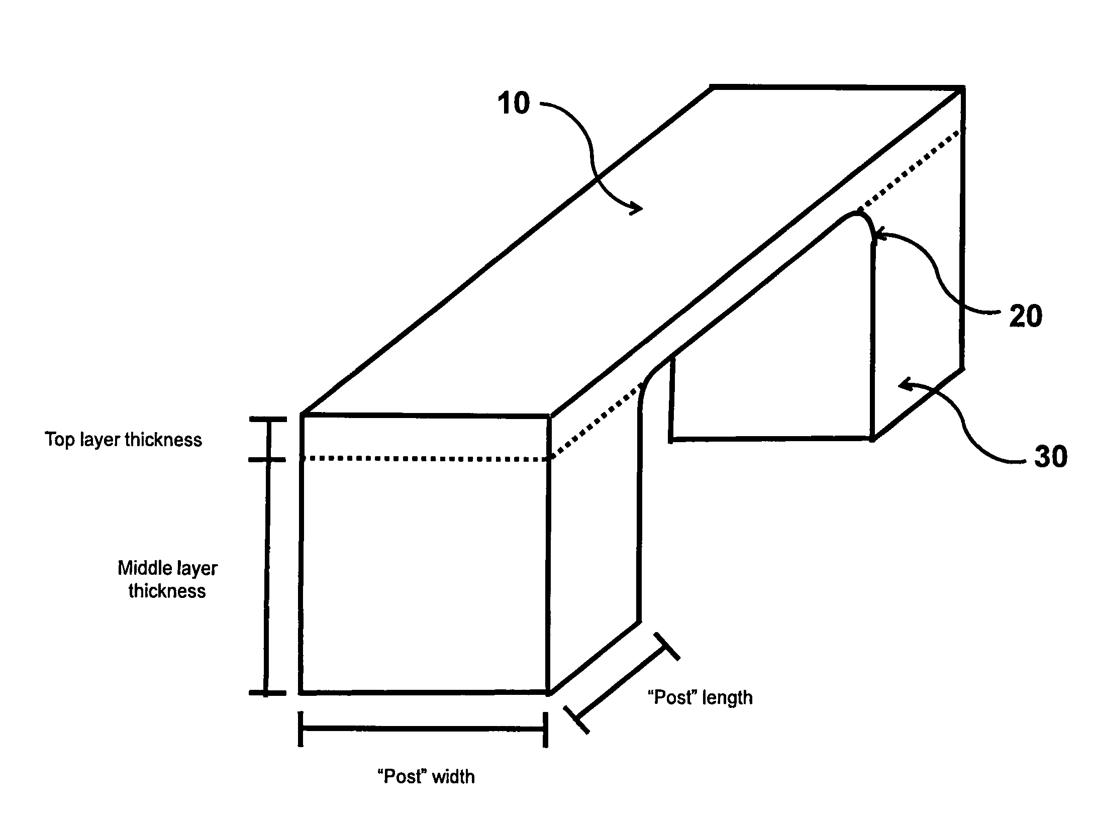
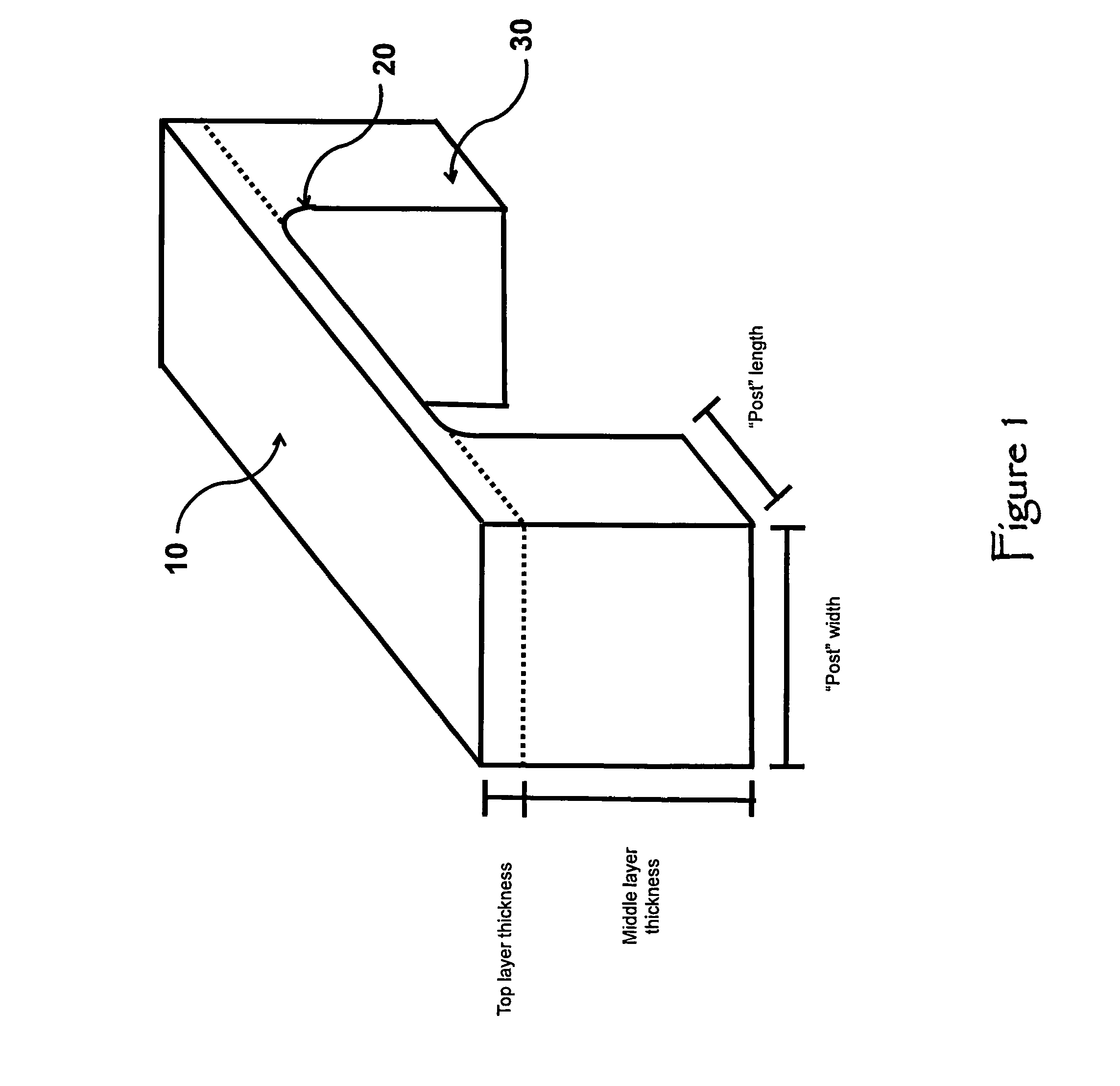
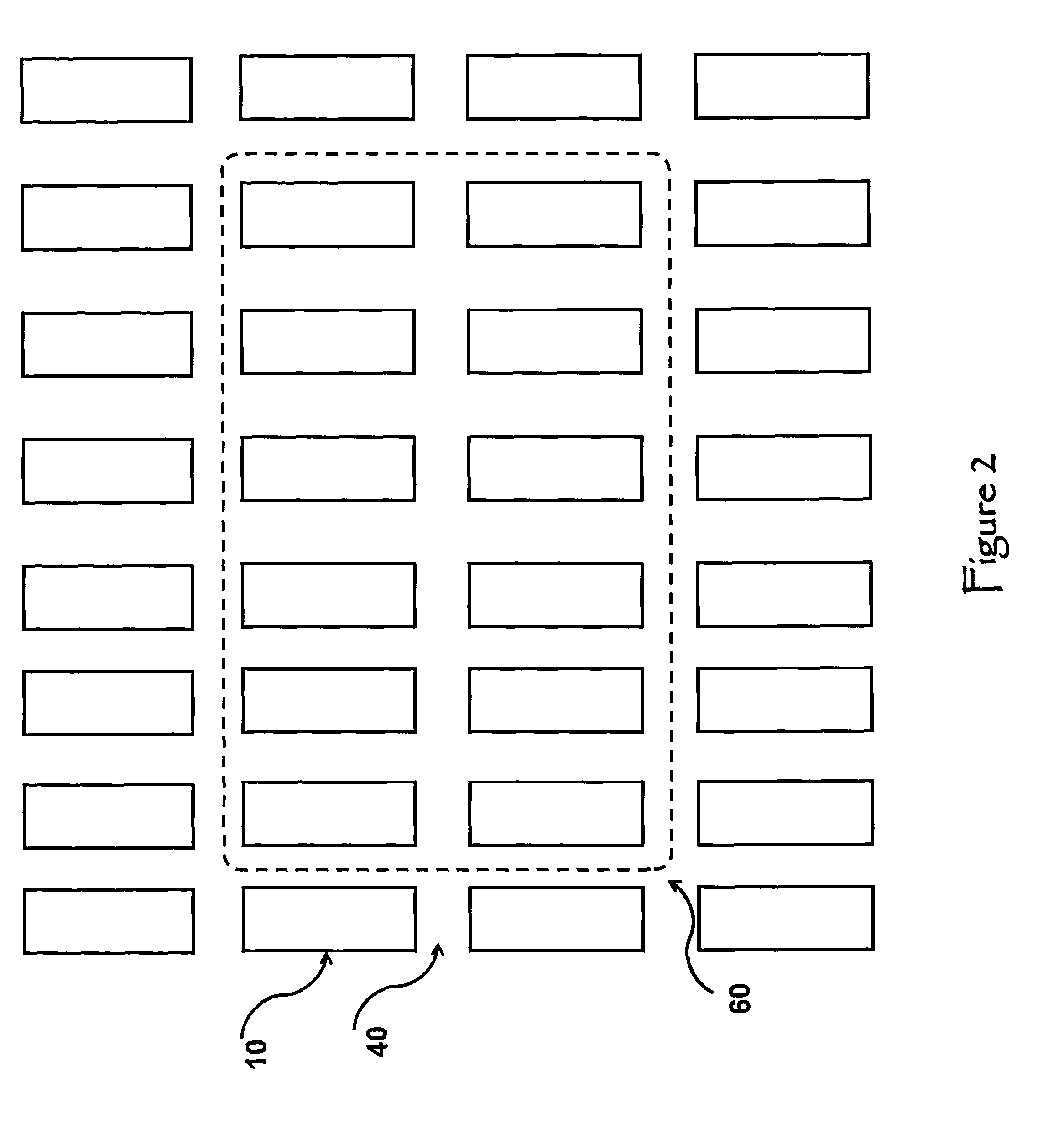
[0035]Referring to FIG. 1, the fundamental detector element 10 is a bridge shaped construction of a superconducting nanowire. A plurality of detector elements 10 will form what is called the detection layer (as depicted FIG. 2). Vertical connections or “posts”30 connect ends of the detector elements 10 to the lead layer via passage ways through the middle insulation layer. Detector elements 10 and vertical connections 30 form a “bridge” and define the bridge's length and height. The length of the bridge and the height of the bridge can be stretched arbitrarily. The thickness of the detector elements 10, or similarly, the thickness of the detection layer, is highly dependent on physical properties of the superconducting material used in the device.

[0036]The minimum length of the detector elements 10 and height of the vertical connections 30 of the “bridge” are determined by the same physical properties of the superconducting material as well at the properties of the insulting materia...


PUM


Abstract

A superconducting nanowire photon detector apparatus comprising detection, insulating, and substrate layers. The insulating layer provides electrical isolation of a plurality of individual detector elements from the interconnection network fabricated on the substrate layer except where electrical interconnection between the inputs and outputs of each detector element and the interconnection network is intended.

Description

PRIORITY CLAIM UNDER 35 U.S.C. §119(e)[0001]This patent application claims the priority benefit of the filing date of provisional application Ser. No. 61 / 631,442, having been filed in the United States Patent and Trademark Office on Dec. 13, 2011 and now incorporated by reference herein.STATEMENT OF GOVERNMENT INTEREST[0002]The invention described herein may be manufactured and used by or for the Government for governmental purposes without the payment of any royalty thereon.BACKGROUND OF THE INVENTION[0003]The ability of a, very thin and very narrow, section or “nanowire” of superconducting material to detect the impact of a photon has long been known. The basic principle is as follows. A nanowire of a superconducting material is created and electrical wired to a voltage source. As the current flows thought the wire it creates heat. If the cooling needed to reach the temperature for superconducting phenomena (TC of approximately 10 kelvin or less) and the heating due to the current...

Claims


Application Information

Patent Timeline
Patent Type & Authority Patents(United States)
IPC IPC(8): G01F23/24
CPCH01L39/10G01J5/023B82Y15/00H10N60/84
Inventor SMITH, AMOS MATTHEW
Owner THE UNITED STATES OF AMERICA AS REPRESETNED BY THE SEC OF THE AIR FORCE
Why Eureka
Try Eureka