Semiconductor integrated circuit including variable resistor circuit

a technology of resistor circuit and integrated circuit, which is applied in the direction of electric variable regulation, process and machine control, instruments, etc., can solve the problems of difficult to trim resistance with accuracy, the trimming amount depends on the on-state resistance of the nmos transistor, and the trimmed resistance has an error, so as to eliminate the power supply voltage dependence and temperature dependence, and reduce the layout area

Active Publication Date: 2013-11-19
ABLIC INC
View PDF7 Cites 0 Cited by
  • Summary
  • Abstract
  • Description
  • Claims
  • Application Information

AI Technical Summary

Benefits of technology

[0009]The present invention has been made in view of the above-mentioned problems, and it is therefore an object thereof to provide a semiconductor integrated circuit including a variable resistor circuit of the small layout area, which is capable of trimming a resistance with accuracy and is free from power supply voltage dependence and temperature dependence.
[0011]Therefore, according to the semiconductor integrated circuit including the variable resistor circuit of the present invention, the ON-state resistances of the switch elements for varying the resistance can be controlled to eliminate an error in trimming amount caused by the ON-state resistances of the switch elements. Besides, the present invention can provide the effect of eliminating the power supply voltage dependence and the temperature dependence and the effect of reducing the layout area.

Problems solved by technology

In the semiconductor integrated circuit including the conventional variable resistor circuit as configured above, there is an error in trimming amount depending on ON-state resistances of the NMOS transistors as switch elements.
It is therefore difficult to trim the resistance with accuracy.
Further, there is another problem that, even if the trimming is performed taking the ON-state resistances into account, the trimmed resistance has an error because of power supply voltage dependence or temperature dependence of the ON-state resistances.
Still further, there is another problem that the layout area of the circuit is increased because it is necessary to increase the size of the NMOS transistors for reducing the ON-state resistances to reduce the influence of the ON-state resistances.

Method used


Image

  • Semiconductor integrated circuit including variable resistor circuit
  • Semiconductor integrated circuit including variable resistor circuit
  • Semiconductor integrated circuit including variable resistor circuit

Examples


first embodiment

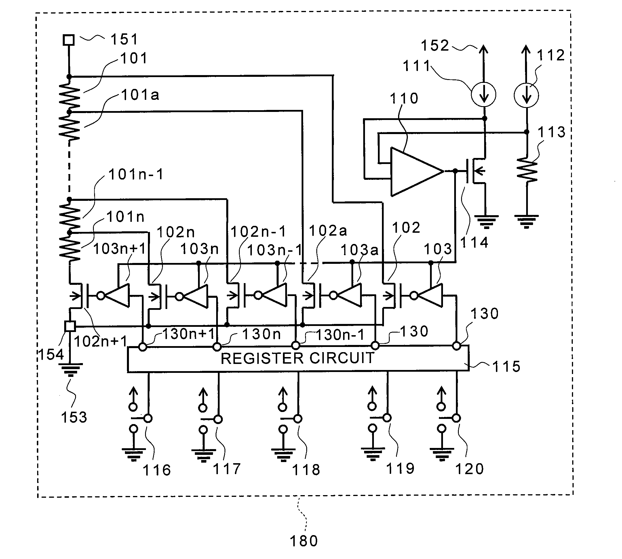
[0021]Next, an operation of the variable resistor circuit 180 as configured above is described.

[0022]Each of the selector switches 116 to 120 is switched in response to an external signal corresponding to a desired resistance, and outputs the switched signal to the register circuit 115. Based on the input signals, the register circuit 115 determines respective signals of the output terminals 130 to 130n+1.

[0023]When Hi is output from the output terminal 130 of the register circuit 115, the output of the inverter 103 is Lo, and the NMOS transistor 102 is turned OFF. When Lo is output from the output terminal 130 of the register circuit 115, the output of the inverter 103 is Hi, and the NMOS transistor 102 is turned ON. The other output terminals and NMOS transistors have the same relationships.

[0024]For example, when Lo is output from the output terminal 130 and Hi is output from all the other output terminals, only the NMOS transistor 102 is turned ON, and hence a resistance betwee...

second embodiment

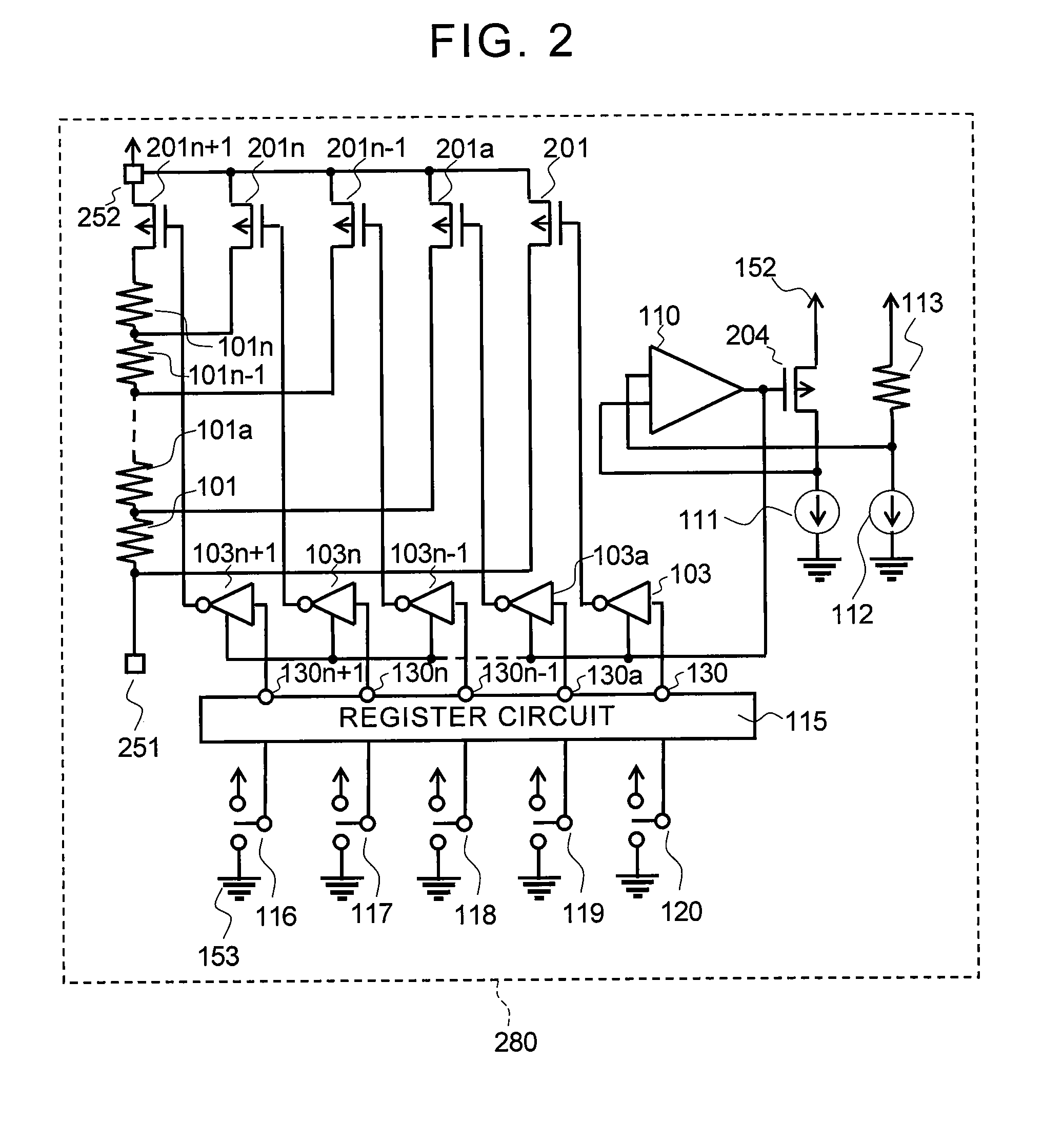
[0034]The amplifier 110 has a non-inverting input terminal connected to the constant current circuit 111 and a drain of the PMOS transistor 204, an inverting input terminal connected to the constant current circuit 112 and one terminal of the resistor 113, and an output connected to a gate of the PMOS transistor 204. The resistor 113 has another terminal connected to a VDD terminal 152. The PMOS transistor 204 has a source connected to the VDD terminal 152. The n resistors 101 to 101n are connected in series, and one end of the n series-connected resistors 101 to 101n is connected to an output terminal 251 and another end thereof is connected to a drain of the PMOS transistor 201n+1. The PMOS transistor 201n+1 has a gate connected to an output of the inverter 103n+1 and a source connected to an output terminal 252. The PMOS transistor 201n has a gate connected to an output of the inverter 103n, a drain connected to a connection point between one terminal of the resistor 101n and one...


PUM


Abstract

Provided is a semiconductor integrated circuit including a variable resistor circuit of the small layout area, which is free from an error in resistance caused by ON-state resistances of switch elements for trimming, and is also free from power supply voltage dependence and temperature dependence. The semiconductor integrated circuit including a variable resistor circuit includes: a resistor circuit including a plurality of series-connected resistors; a selection circuit including a plurality of switch elements for selecting a connected number of the plurality of series-connected resistors; and a control circuit for controlling ON-state resistances of the plurality of switch elements. The control circuit controls the ON-state resistances of the plurality of switch elements so as to obtain a predetermined ratio to a resistance of the plurality of series-connected resistors of the resistor circuit.

Description

RELATED APPLICATIONS[0001]This application claims priority under 35 U.S.C. §119 to Japanese Patent Application No. 2010-133266 filed on Jun. 10, 2010, the entire content of which is hereby incorporated by reference.BACKGROUND OF THE INVENTION[0002]1. Field of the Invention[0003]The present invention relates to a semiconductor integrated circuit including a variable resistor circuit.[0004]2. Description of the Related Art[0005]FIG. 3 illustrates a semiconductor integrated circuit including a conventional variable resistor circuit. Referring to FIG. 3, a trimming circuit 351 includes PMOS transistors 310, 311, and 312, NPN transistors 313, 314, and 315, constant current sources 316, 317, and 318, control signal input pads 321, 322, and 323, and wirings D, E, and F. The PMOS transistors 310, 311, and 312 each have a source connected to a VDD terminal and a gate connected to a control terminal VG. The NPN transistor 313 has a base connected to the constant current source 316 and the con...

Claims


Application Information

Patent Timeline
Patent Type & Authority Patents(United States)
IPC IPC(8): H03L5/00
CPCG05F1/561H01C1/16H01C10/50H01L21/768H01L27/00
Inventor UTSUNOMIYA, FUMIYASU
Owner ABLIC INC
Why Eureka
Try Eureka