Top-gate transistor array substrate

a transistor array and substrate technology, applied in the field of transistor array substrates, can solve the problems of reducing achieve the effects of preventing the formation of oxygen vacancy, improving the reliability of the lcd, and avoiding the change of the resistance of the mos layer

Inactive Publication Date: 2013-12-24
CHUNGHWA PICTURE TUBES LTD +1
View PDF7 Cites 0 Cited by
  • Summary
  • Abstract
  • Description
  • Claims
  • Application Information

AI Technical Summary

Benefits of technology

[0015]According to an embodiment of the present invention, the pixel array further comprises: a plurality of first conductive columns disposed in the second insulating layer and connected between the pixel electrodes and the drains; and a plurality of second conductive columns, disposed in the second insulating layer and connected between the data lines and the sources. Based on the foregoing, since the MOS layer contacts the ion release layer, the ion release layer can release a plurality of ions into the MOS layer, so as to inhibit the formation of oxygen vacancy in the MOS layer. Thus, the change of the resistance of the MOS layer is avoided, thereby improving the reliability of the LCD.

Problems solved by technology

Once too many oxygen ions move towards the gate, the resistance of the MOS layer will change, and it influences the operation of the LCD, thereby resulting in decrease of the reliability of the LCD.

Method used


Image

  • Top-gate transistor array substrate
  • Top-gate transistor array substrate

Examples


Embodiment Construction

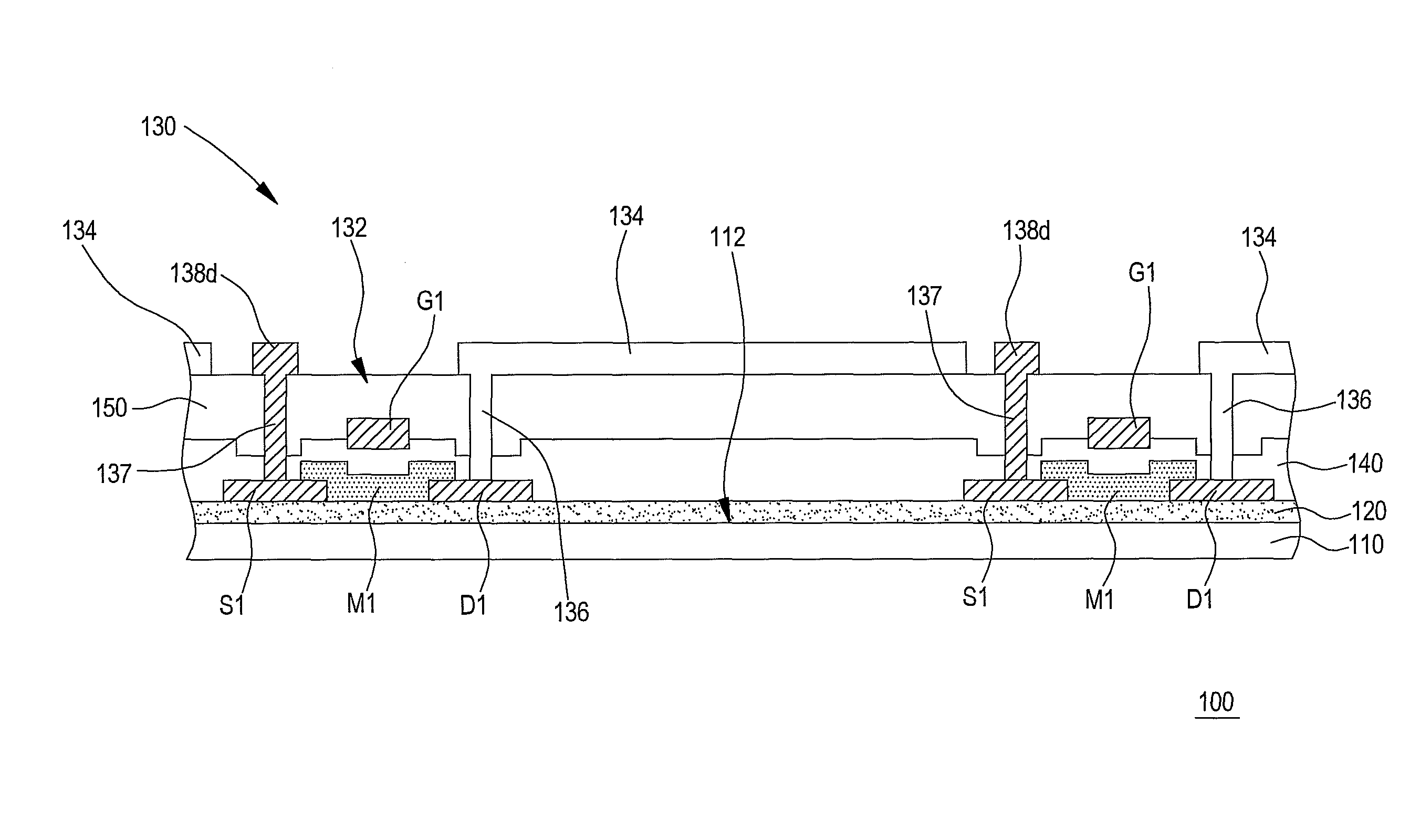
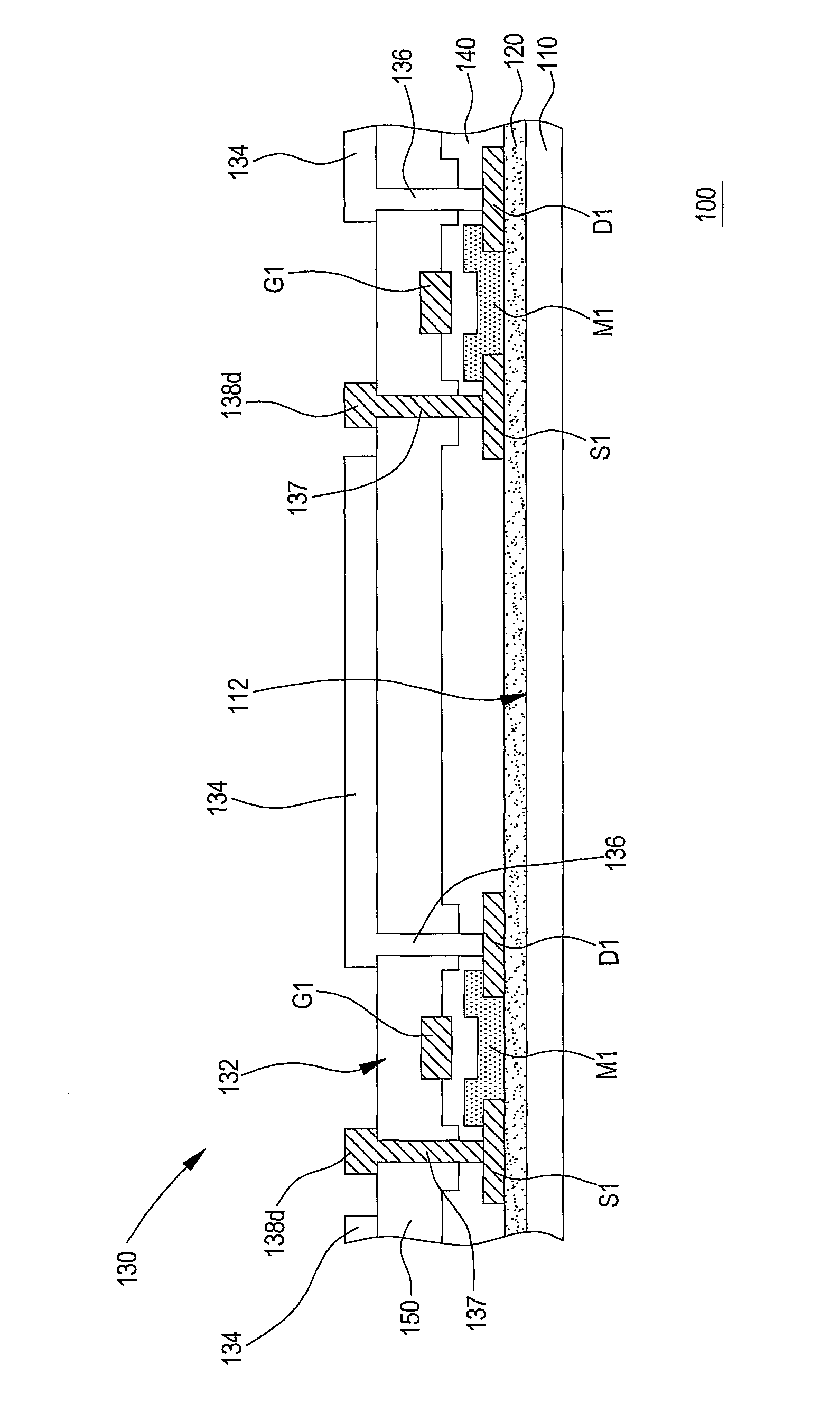
[0019]FIG. 1 is a schematic cross-sectional view of a top-gate transistor array substrate according to an embodiment of the present invention. Referring to FIG. 1, a top-gate transistor array substrate 100 of this embodiment includes a transparent substrate 110, an ion release layer 120 and a pixel array 130. The transparent substrate 110 has a plane 112, and the ion release layer 120 is disposed on the transparent substrate 110 and completely covers the plane 112.

[0020]The pixel array 130 is disposed on the ion release layer 120, and includes a plurality of transistors 132 and a plurality of pixel electrodes 134. The pixel electrodes 134 are electrically connected to the transistors 132 respectively. The pixel electrodes 134 may be transparent conductive films, and the material of the pixel electrode 134 is, for example, indium tin oxide (ITO) or indium zinc oxide (IZO).

[0021]Each of the transistors 132 is a MOS field effect transistor (MOSFET), so each of the transistors 132 inclu...


PUM


Abstract

A top-gate transistor array substrate includes a transparent substrate with a plane, an ion release layer, a pixel array, and a first insulating layer. The ion release layer is disposed on the transparent substrate and completely covers the plane. The pixel array is disposed on the ion release layer and includes a plurality of transistors and a plurality of pixel electrodes. Each of the transistors includes a source, a drain, a gate and a MOS (metal oxide semiconductor) layer. The drain, the source and the MOS layer are disposed on the ion release layer. The pixel electrodes are electrically connected to the drains respectively. The gate is disposed above the MOS layer. The first insulating layer is disposed between the MOS layers and the gates. The MOS layer contacts the ion release layer. The ion release layer can release a plurality of ions into the MOS layers.

Description

CROSS-REFERENCE TO RELATED APPLICATION[0001]This application claims the benefit of Taiwan Patent Application No. 100212279, filed on Jul. 5, 2011, which is hereby incorporated by reference for all purposes as if fully set forth herein.BACKGROUND OF THE INVENTION[0002]1. Field of Invention[0003]The present invention relates to a transistor array substrate, and more particularly, to a top-gate transistor array substrate.[0004]2. Related Art[0005]Currently, a liquid crystal display (LCD) with a metal oxide semiconductor (MOS) layer is present. The thin-film transistor (TFT) of the LCD has an active layer made of MOS. When the LCD is in operation, a positive voltage is applied to a gate of the TFT to enable the gate to generate an electric field.[0006]A plurality of oxygen ions (O2−) in the semiconductor layer are driven by the electric field and move towards the gate. When the oxygen ions move towards the gate, an oxygen vacancy occurs in the MOS layer. That is to say, the regions lack...

Claims


Application Information

Patent Timeline
Patent Type & Authority Patents(United States)
IPC IPC(8): H01L29/10
CPCH01L27/1225H01L29/78603H01L29/78606H01L29/7869
Inventor CHENG, HUANG-CHUNGHUANG, YU-CHIHYANG, PO-YUCHIANG, SHIN-CHUANLI, HUAI-AN
Owner CHUNGHWA PICTURE TUBES LTD
Why Eureka
Try Eureka