Vertically integrated optical phased array with pseudo-random array architecture

a phased array and array technology, applied in semiconductor lasers, electrical devices, laser details, etc., can solve the problems of limited temperature range of operation, grating lobes, slow steering speed (10's of ms range), etc., and achieve the effect of reducing grating lobes

Active Publication Date: 2013-12-24
HRL LAB
View PDF5 Cites 23 Cited by
  • Summary
  • Abstract
  • Description
  • Claims
  • Application Information

AI Technical Summary

Benefits of technology

[0010]In another aspect this invention provides method of forming reducing grating lobes in an optical phased array, the method including: providing a plurality of vertical cavity surface emitting lasers; providing a plurality of vertical cavity phase modulators, with individual modulators of said plurality of vertical cavity phase modulators each being disposed in optical alignment with an injection port of a corresponding one of s

Problems solved by technology

The presence of grating lobes is one of the main issues with prior art optical phased arrays due to the difficulty of fabricating arrays with spacings less than wavelength.
However, the main issue with the LC-OPA is its slow steering speed (10's of ms range) which is due to the slow response time of the LC-based phase shifting elements.
Another disadvantage of liquid crystals is their limited temperature range of operation.
At low temperatures (50° C.) it becomes isotropic and hence loses its functionality.
The main problem with this approach is that it is mainly a 1-D phased array.
2-D beam steering can be achieved by placing tunable waveguide gratings at the end of the phase shifters, but scanning in the elevatio

Method used


Image

  • Vertically integrated optical phased array with pseudo-random array architecture
  • Vertically integrated optical phased array with pseudo-random array architecture
  • Vertically integrated optical phased array with pseudo-random array architecture

Examples


Embodiment Construction

[0018]The key features of the prior art optical phased arrays and the novel V-OPA device disclosed herein are compared in the Table below.

[0019]

Waveguide Self-Locked OPAOPA TechnologyV-OPAVCSELsLC-OPAOPAOPA Dimension2221Beam Scanning >10 msSpeedPhase shift per 2π2πelement(cm long WG)Grating LobesNoYesYesYesMode hoppingNoYesN / ANoIndep. phase / amp YesNoNoYescontrol

[0020]Overview of the V-OPA Device and the Manufacture of Same

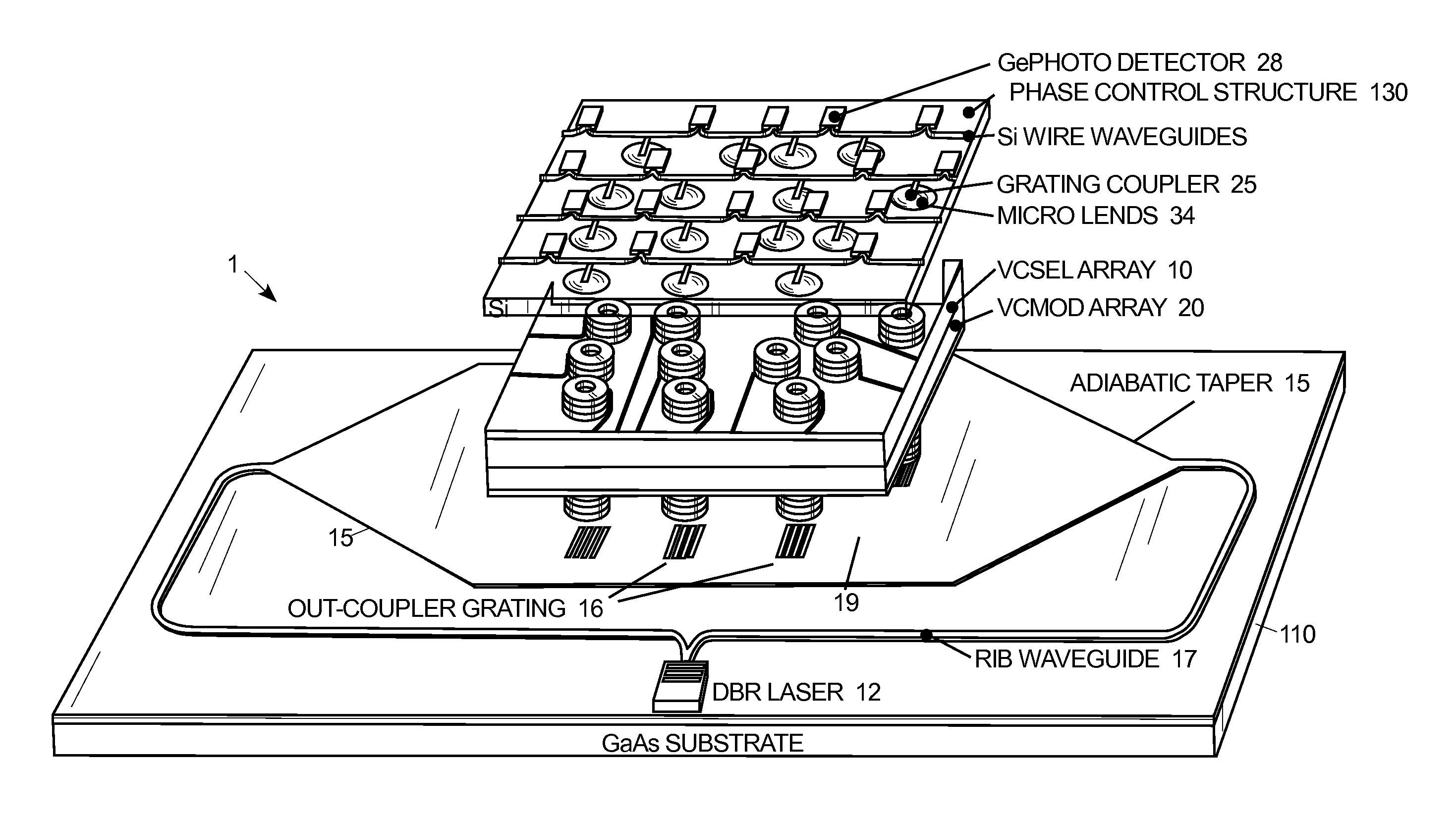
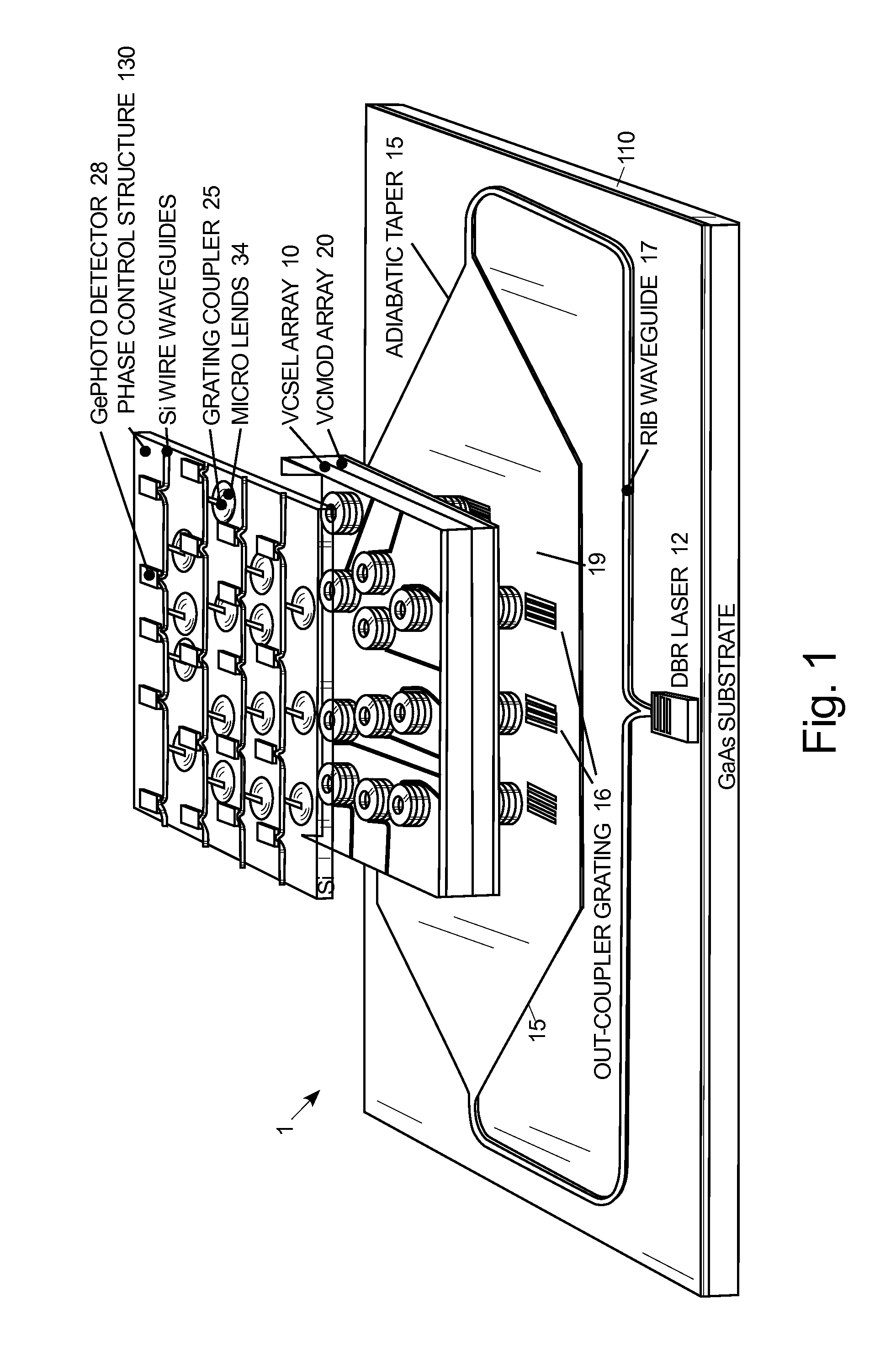
[0021]A schematic diagram of a preferred embodiment the V-OPA device 1 is shown in FIG. 1 as a perspective view thereof. The various device layers are intentionally displaced in the vertical direction for better visualization of their structure The V-OPA device 1 of the present invention is proposed to preferably consist of four main functional layers:

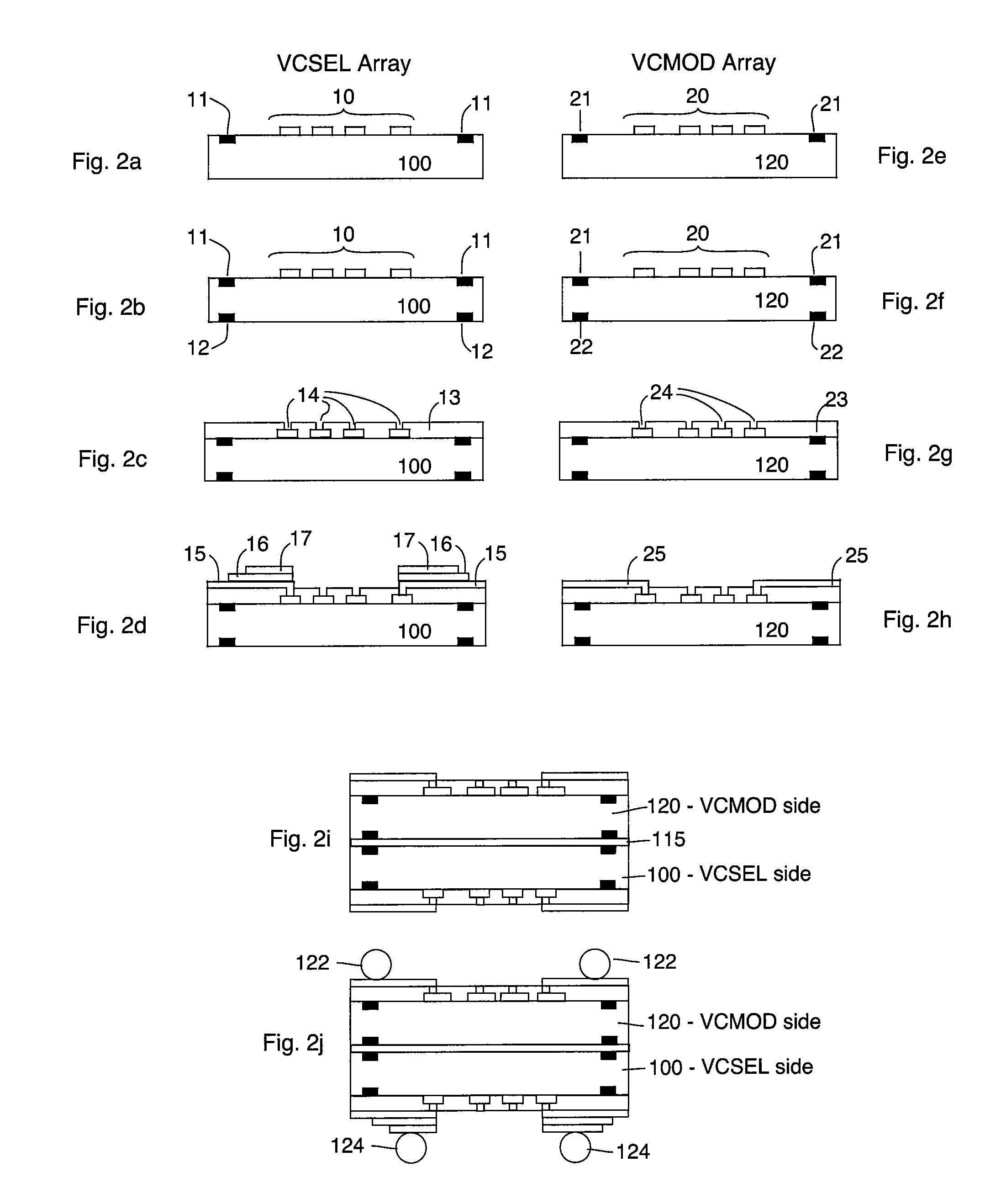
[0022](1) A 2-D array of vertical cavity surface emitting lasers (VCSELs) 10, preferably with a wall-plug efficiency of >40%, for generating emitting optical beamlets 18 of the phased array (see FIG. 2s). The VCSELs 1...


PUM


Abstract

A vertically integrated optical phased array has an array of a plurality of vertical cavity surface emitting lasers disposed in an aperiodic arrangement thereof, the plurality of vertical cavity surface emitting lasers having light emitting ports disposed parallel to one another. An array of a plurality of vertical cavity phase modulators disposed in the same aperiodic arrangement as the array of the plurality of vertical cavity surface emitting lasers, with individual modulators of said array of a plurality of vertical cavity phase modulators each being disposed in optical alignment with an injection port of a corresponding one of said plurality of vertical cavity surface emitting lasers. An array of a plurality of laser ports, fed by a master laser, are disposed in the same aperiodic arrangement as the array of the plurality of vertical cavity surface emitting lasers, the master laser providing, in use, injection beamlets, each injection beamlet, in use, injection locking a corresponding one of said plurality of vertical cavity surface emitting lasers via a corresponding one of said plurality of vertical cavity phase modulators.

Description

CROSS REFERENCE TO RELATED APPLICATIONS[0001]NoneTECHNICAL FIELD[0002]This invention relates to a chip-scale optical phased array (OPA) device, based on vertical integration of a 2-D aperiodic array of pseudo-randomly placed (p-random) vertical cavity surface emitting lasers (VCSEL), with a corresponding 2-D array of coherent phase modulating optical injection beams.BACKGROUND[0003]Optical phased array (OPA) device are known in the prior art, but they have grating lobes in their output beams.[0004]The presence of grating lobes is one of the main issues with prior art optical phased arrays due to the difficulty of fabricating arrays with spacings less than wavelength. This problem is overcome by the present invention. The present invention provides additional benefits, including a narrow beamwidth of the output beam together with high beam position accuracy.[0005]The prior art includes a liquid crystal-based optical phased array (LC-OPA) which consists of a liquid crystal (LC) cell w...

Claims


Application Information

Patent Timeline
IPC IPC(8): H01S5/00
CPCH01S5/4006H01S5/423H01S5/0085H01S5/026H01S5/18302H01S5/06246H01S2301/20
Inventor SAYYAH, KEYVANSCAFFNER, JAMES H.WHITE, CARSON R.
Owner HRL LAB
Why Eureka
Try Eureka