Signal measuring device and signal measuring method

a signal measuring and signal technology, applied in the direction of instruments, pulse manipulation, pulse technique, etc., can solve the problems of difficult to readily estimate malfunction, noise, clock fluctuation (jitter) and temperature variations, and increase in the case of chip malfunction, so as to achieve satisfactory precision and estimate the measurement time

Inactive Publication Date: 2014-01-21
NEC CORP
View PDF13 Cites 4 Cited by
  • Summary
  • Abstract
  • Description
  • Claims
  • Application Information

AI Technical Summary

Benefits of technology

[0017]It is an object of the present invention to provide a signal measuring device and signal measuring method that make it possible to estimate measurement time with satisfactory precision at low-speed operation.
[0039]In accordance with the present invention, measurement timing is identified using a reference signal having a speed lower than that of a driving clock signal for measurement. As a result, it possible to estimate measurement time with satisfactory precision using a reference signal having an operating frequency that is low in comparison with the prior art.

Problems solved by technology

Furthermore, with advances that have been made in lowering voltage, there has been a remarkable increase in cases in which noise, clock fluctuation (jitter) and temperature variations, etc., give rise to chip malfunction.
Further, owing to the higher integration that accompanies microfabrication, behavior within the chip is becoming increasingly complex and it has become difficult to readily estimate malfunction.
As the operating frequency of the integrated circuit rises, noise and jitter, etc., having high-frequency components increase.
As a consequence, it is difficult to observe noise and jitter within an integrated circuit accurately outside the integrated circuit.
Further, in cases where a signal or clock is sampled externally of an integrated circuit, noise and jitter produced in the course of extracting the signal or clock to the exterior of the integrated circuit occur in addition to the noise and jitter produced within the integrated circuit.
This makes it difficult to estimate noise and jitter accurately at the point of measurement.
If result of measurement is retained in such a device, there is the danger that the amount of storage will be very great.
Further, in a case where there is need for counter values in a number equivalent to the number of measurement cycles, the number of bits necessary for the identification signal increases and circuit timing design becomes more difficult.
In particular, in cases where the driving clock signal takes on a near-gigahertz frequency, jitter and frequency fluctuation increase and it becomes difficult to estimate measurement time with satisfactory precision.

Method used


Image

  • Signal measuring device and signal measuring method
  • Signal measuring device and signal measuring method
  • Signal measuring device and signal measuring method

Examples


first exemplary embodiment

(Method of storing all measurement data in memory in order)

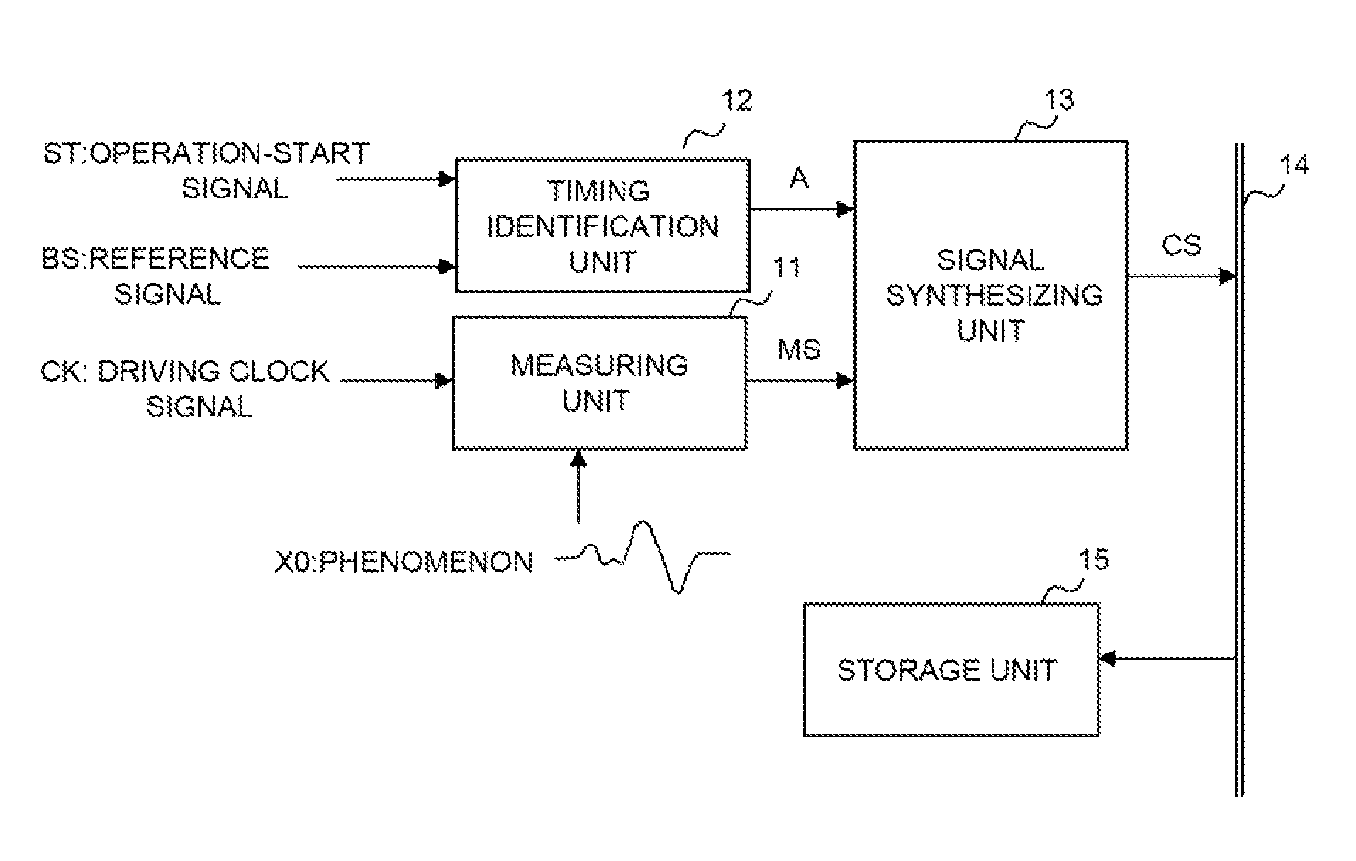
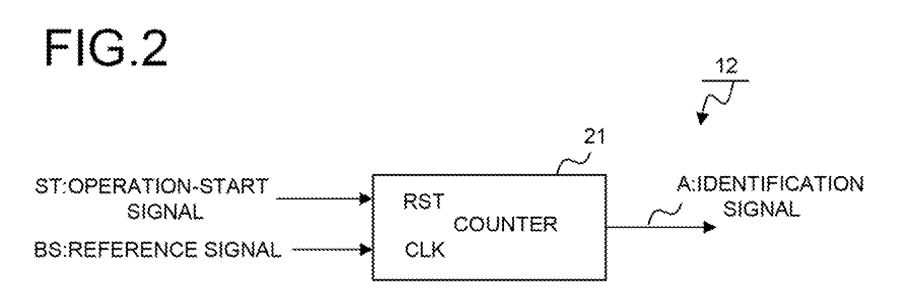
[0078]FIG. 1 is a block diagram illustrating the configuration of a signal measuring device according to a first exemplary embodiment of the present invention. The signal measuring device in FIG. 1 includes a measuring unit 11, a timing identification unit 12, a signal synthesizing unit 13, a data bus 14 and a storage unit 15. The measuring unit 11 measures a phenomenon X0 in synch with a driving clock signal CK that is for measuring purposes and outputs a measurement result every period of the driving clock signal CK as a measurement-result signal MS. Meanwhile, the timing identification unit 12, which identifies the timing at which the measuring unit 11 operates, receives as inputs an operation-start signal ST, which is used as timing for starting the output of measurement data, and a reference signal BS that rises at a fixed period, and outputs an identification signal A. The signal synthesizing unit 13 generates a synthe...

second exemplary embodiment

Method of Storing Random Data of Measurement Data

[0089]The configuration of the signal measuring device according to the second exemplary embodiment of the present invention is similar to that shown in FIG. 1. However, the internal configuration of the timing identification unit 12 is different. The signal measuring device according to the second exemplary embodiment is illustrated with regard to a case where the measurement-result signals MS of all periods are stored in the storage unit 15 in FIG. 1 but no limitation is applied with respect to the order in which the data is written to the storage unit 15, i.e., the data is stored at addresses in the storage unit 15 in an order different from the order of generation, as illustrated in FIG. 10. When the stored synthesized signals are read out in this case, the data generation timing cannot be identified in order from the leading bit by the method shown in FIG. 5 if the order in which the measurement-result signals MS were generated c...

third exemplary embodiment

Method of Storing Some Measurement Data in Memory

[0096]FIG. 16 is a block diagram illustrating the configuration of a signal measuring device according to a third exemplary embodiment of the present invention. Components in FIG. 16 identical with those shown in FIG. 1 are designated by like reference characters and are not described again. A comparator 16 senses whether the measurement-result signal MS is outside the range of a reference value RE set in advance. If the measurement-result signal MS is outside the range of the reference value RE, i.e., if it is recognized that phenomenon X0 is abnormal, this fact is reported to an output controller 17. The output controller 17 transfers the synthesized signal CS, which is output by the signal synthesizing unit 13, to the storage unit 15 only in a case where phenomenon X0 is abnormal. If this arrangement is adopted, the overall number of items of data stored in the storage unit 15 can be reduced and a reduction in the amount of memory ...


PUM


Abstract

A signal measuring device, comprises one set, or a plurality of sets, of measuring unit(s) measuring an object of measurement in synch with a driving clock signal for measurement and outputting result of measurement as first data, and a timing identification unit which, in accordance with a measurement-start command, outputs a value, which differs every period, as second data in synch with a reference signal having a prescribed period and a speed lower than that of the driving clock signal; and a storage unit collecting and successively storing the first data and the second data as one set in synch with the driving clock signal.

Description

[0001]This application is the National Phase of PCT / JP2007 / 074396 filed Dec. 19, 2007, which claims the benefit of previous Japanese Patent Application No, 2006-344648 (filed on Dec. 21, 2006), which is hereby incorporated by reference herein in its entirety.TECHNICAL FIELD[0002]The present invention relates to a signal measuring device and signal measuring method. More particularly, the invention relates to a technique for identifying the output timing of a measurement-result signal in a semiconductor integrated circuit device.BACKGROUND ART[0003]Power supply noise generated within a semiconductor integrated circuit device (LSI) is increased by microfabrication within the LSI chip and by higher speed. Furthermore, with advances that have been made in lowering voltage, there has been a remarkable increase in cases in which noise, clock fluctuation (jitter) and temperature variations, etc., give rise to chip malfunction. Further, owing to the higher integration that accompanies micro...

Claims


Application Information

Patent Timeline
Patent Type & Authority Patents(United States)
IPC IPC(8): G01R13/02
CPCG01R31/31937G01R31/31708G01R31/31726
Inventor NOSE, KOICHIMIZUNO, MASAYUKISHIBAYAMA, ATSUFUMI
Owner NEC CORP
Why Eureka
Try Eureka