Light emitting diode (LED) using three-dimensional gallium nitride (GaN) pillar structures with planar surfaces

a technology of gallium nitride and light-emitting diodes, which is applied in the direction of semiconductor/solid-state device manufacturing, electrical equipment, semiconductor devices, etc., can solve the problems of limiting the range of emission characteristics that are achievable, affecting device performance and reliability, and high cost of producing gans for devices. achieve the effect of improving performance, increasing emission area, and high efficiency

Active Publication Date: 2014-02-11
ELUX INC
View PDF16 Cites 30 Cited by
  • Summary
  • Abstract
  • Description
  • Claims
  • Application Information

AI Technical Summary

Benefits of technology

[0015]Disclosed herein is a class of structures for gallium nitride (GaN) based light emitting diodes (LEDs) that have improved performance because of the 3-dimensional shape of the initial GaN template over which the LED layers are deposited. The template shape can be columnar, which forms micro-rod or pillar LEDs, and can be connected in an array to make high efficiency lighting of arbitrary size and shape. Alternatively, the template can have a series of pits that increase the emission area and improve light extraction for a planar device. Template shapes are formed by a combination of a damage etch and a wet etch that selectively removes damaged GaN, leaving high quality low etch rate crystalline planes. LED devices made from these template shapes are unlike conventional technologies that fabricate LED structures by MOCVD deposition on planar n-type GaN substrates, creating large planar devices. Further, unlike conventional devices, LED devices made from the above-mentioned templates do not require addition top surface texturing after the LED device is formed.

Problems solved by technology

One of the constraints on this technology is the high cost of producing GaN for devices due to the difficulties encountered in forming a sufficient high-quality material.
These difficulties primarily stem from the growth process, which is typically conducted at very high temperatures (e.g., over 1,000° C.) in molecular beam epitaxy (MBE) or MOCVD reactors and on substrates with a different coefficient of thermal expansion (CTE).
The difference in CTE can lead to formation of threading dislocations that adversely affect device performance and reliability.
In addition, film stress limits the amount of dopants that can be incorporated in a GaN film, which in turn limits the range of emission characteristics that are achievable.
Light outside the escape cone is reflected internally, diminishing the efficiency of the device.
However, the growth was limited to 2 μm per hour.
The crystallographic orientation of VLS-grown GaN nanowires can be non-ideal, as there are competing preferred axial orientations for growth (a- and c-axis, depending on temperature), competing phases (zinc-blend and wurtzite), and the resulting nanowires can have non-uniform sidewall orientations.

Method used


Image

  • Light emitting diode (LED) using three-dimensional gallium nitride (GaN) pillar structures with planar surfaces
  • Light emitting diode (LED) using three-dimensional gallium nitride (GaN) pillar structures with planar surfaces
  • Light emitting diode (LED) using three-dimensional gallium nitride (GaN) pillar structures with planar surfaces

Examples


Embodiment Construction

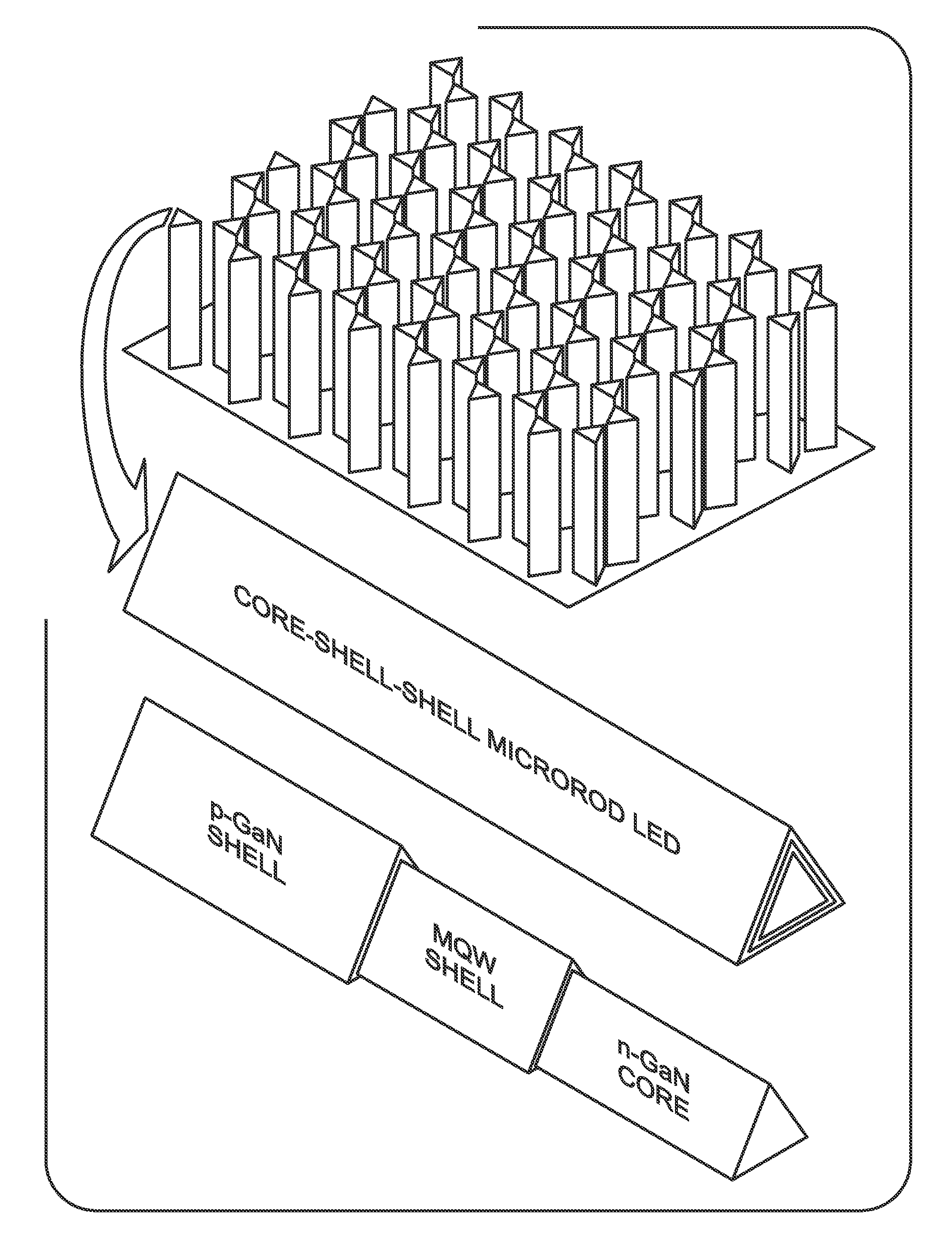
[0039]FIGS. 4A and 4B are partial cross-sectional views of a GaN three-dimensional (3D) structure. The GaN 3D structure 400 comprises a GaN pillar 402 and pillar sidewalls 404. The pillar sidewalls 404 are formed in either the m-plane (10 10) or a-plane ( 12 10). Each family of planes (m and a) both contain 6 faces. The 6 faces for the m-plane family are {10 10}, { 1010}, {01 10}, {0 110}, {1 100}, and { 1100}. For the a-plane family, the faces are {1 210}, { 12 10}, {11 20}, {2 110}, { 1120}, and { 2110}. Note that for these Miller indices, families are in (parentheses), faces are in {curly brackets}, and zone axes are in [square brackets]. As shown in FIG. 4B, the GaN pillar 402 has a triangular pattern. However, hexagonally shaped pillars may alternatively be formed, see FIG. 6B.

[0040]FIG. 5 is a partial cross-section view depicting a GaN 3D array. The array 500 comprises a substrate 502 with a top surface 504, with an array of GaN structures 506. Each GaN structure 506 has a fir...


PUM


Abstract

A method is provided for fabricating a light emitting diode (LED) using three-dimensional gallium nitride (GaN) pillar structures with planar surfaces. The method forms a plurality of GaN pillar structures, each with an n-doped GaN (n-GaN) pillar and planar sidewalls perpendicular to the c-plane, formed in either an m-plane or a-plane family. A multiple quantum well (MQW) layer is formed overlying the n-GaN pillar sidewalls, and a layer of p-doped GaN (p-GaN) is formed overlying the MQW layer. The plurality of GaN pillar structures are deposited on a first substrate, with the n-doped GaN pillar sidewalls aligned parallel to a top surface of the first substrate. A first end of each GaN pillar structure is connected to a first metal layer. The second end of each GaN pillar structure is etched to expose the n-GaN pillar second end and connected to a second metal layer.

Description

RELATED APPLICATIONS[0001]This application is a Continuation-in-Part of a pending application entitled, METHOD FOR FABRICATING THREE-DIMENSIONAL GALLIUM NITRIDE STRUCTURES WITH PLANAR SURFACES, invented by M. Albert Crowder et al., Ser. No. 13 / 337,843, filed Dec. 27, 2011, which is incorporated herein by reference.BACKGROUND OF THE INVENTION[0002]1. Field of the Invention[0003]This invention generally relates to light emitting diode (LED) fabrication processes and, more particularly, to a method for fabricating three-dimensional (3D) gallium nitride structures with planar surfaces for use in LEDs.[0004]2. Description of the Related Art[0005]FIG. 1 is a partial cross-sectional view of a planar gallium nitride LED (prior art). Gallium nitride (GaN) is widely used for LED applications due to its favorable band-gap and direct band structure, and most fabrication follows a planar metalorganic chemical vapor deposition (MOCVD) sequence, as noted by Nguyen, X. L., Nguyen, T. N. N., Chau, V...

Claims


Application Information

Patent Timeline
Patent Type & Authority Patents(United States)
IPC IPC(8): H01L33/04
CPCH01L33/32H01L33/18H01L33/24H01L33/0075H01L33/04H01L33/06H01L33/08H01L33/42H01L2933/0008H01L2933/0016H01L24/95H01L25/0753H01L33/005H01L33/0095H01L2224/95085H01L2224/95136H01L2924/10156H01L2924/12041H01L2933/0033H01L2224/49107H01L2224/48463H01L2924/00012
Inventor CROWDER, MARK ALBERTZHAN, CHANGQINGSCHUELE, PAUL J.
Owner ELUX INC
Why Eureka
Try Eureka